
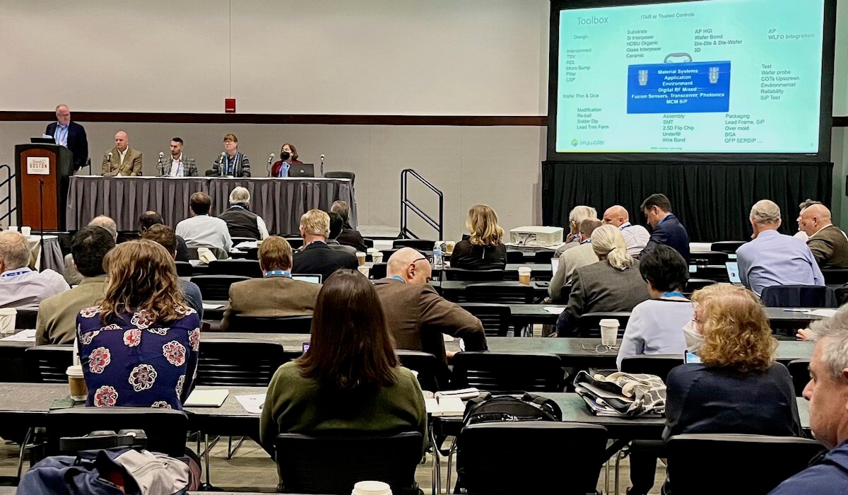
As we noted in IFTLE 537, prior to the 2022 IMAPS conference in Boston earlier this month, IMAPS hosted a one-day workshop on “On-Shore Packaging and Assembly Capabilities” to engage the community and identify solutions to address US government and defense requirements that are critical to the onshoring of the microelectronic assembly and packaging supply chain.
One of the speakers in the workshop was Tomoyuki Yamada of Kyocera who spoke on the topic of “Organic Substrate Process and Commercial Practice”. As you may recall, high-density build-up substrates (HDBU) are one of the technology areas the DoD is very interested in, in terms of bringing technology back on shore.
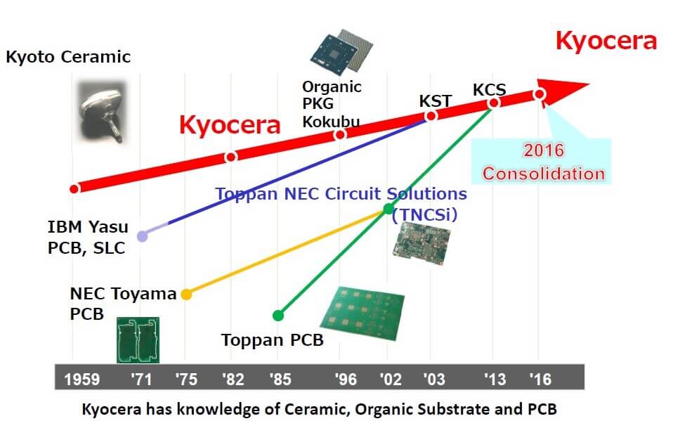
History of HDBU
This presentation had some very insightful info that I want to cover for you in detail. You may not know that Kyocera, once solely a ceramic company, has been acquiring board and substrate capability since 2003 when it acquired the IBM Yasu SLC business. IBM SLC was the first commercial HDBU technology.
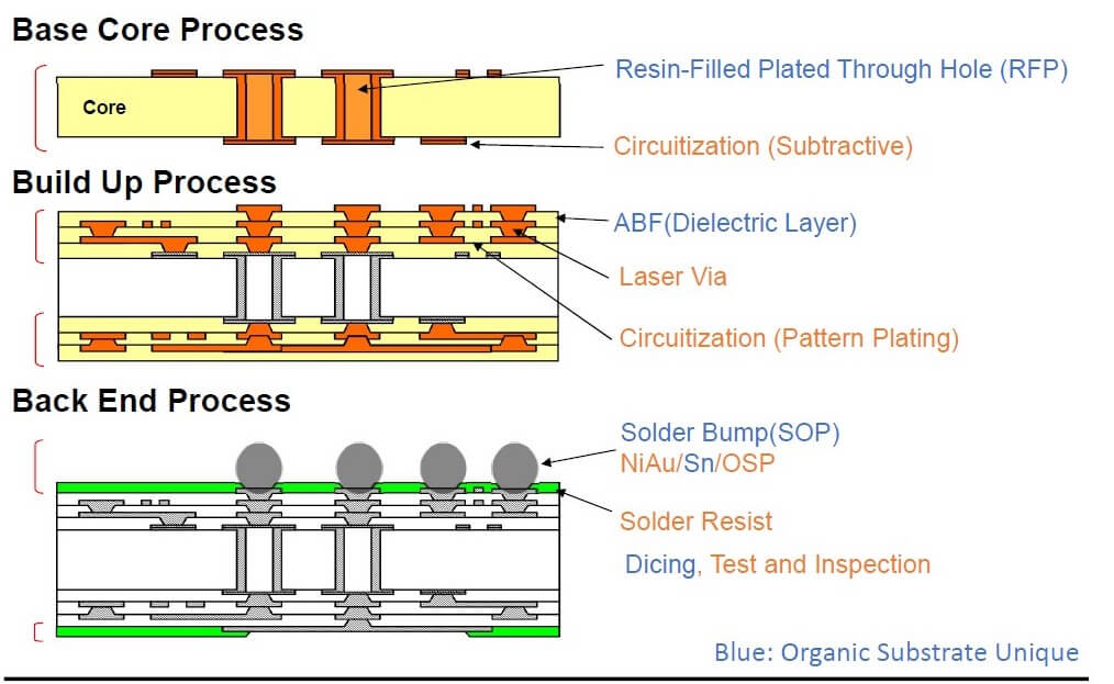
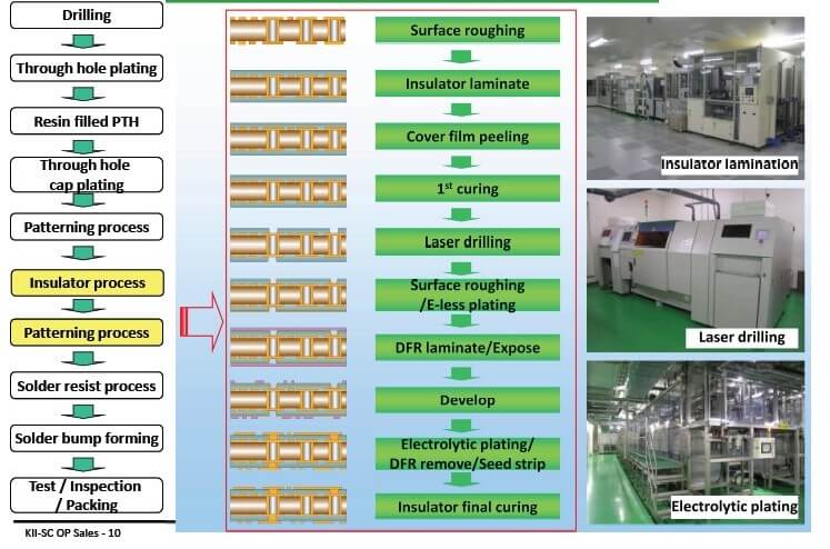
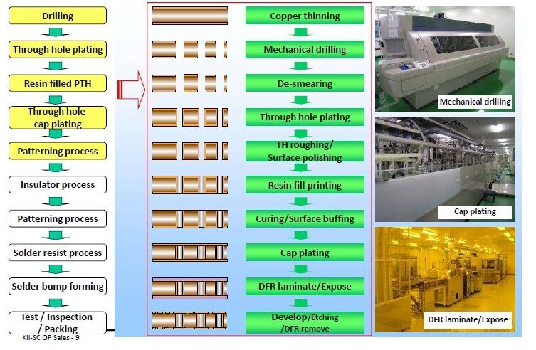
The process flow for organic substrates is shown in Figure 2.
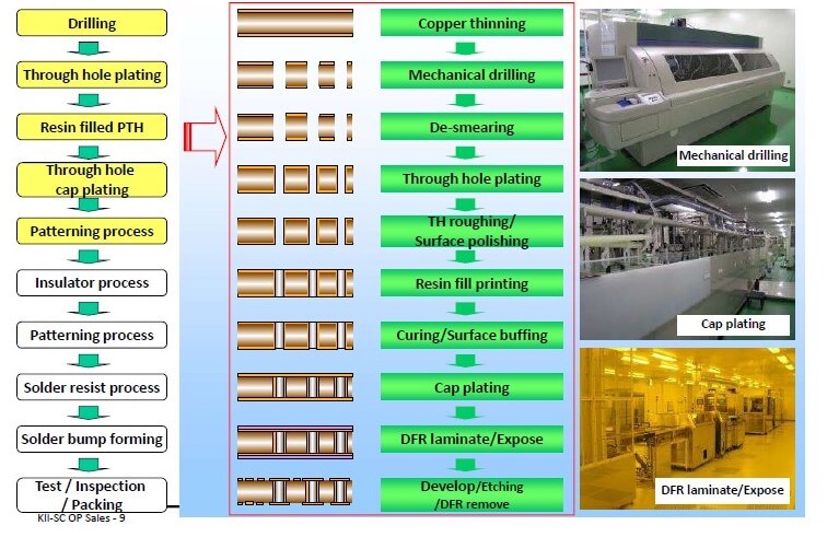
Examination of the process flow in more detail is shown in Figures 3-5.
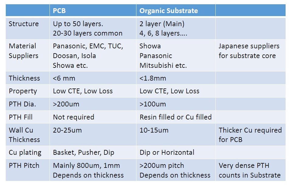
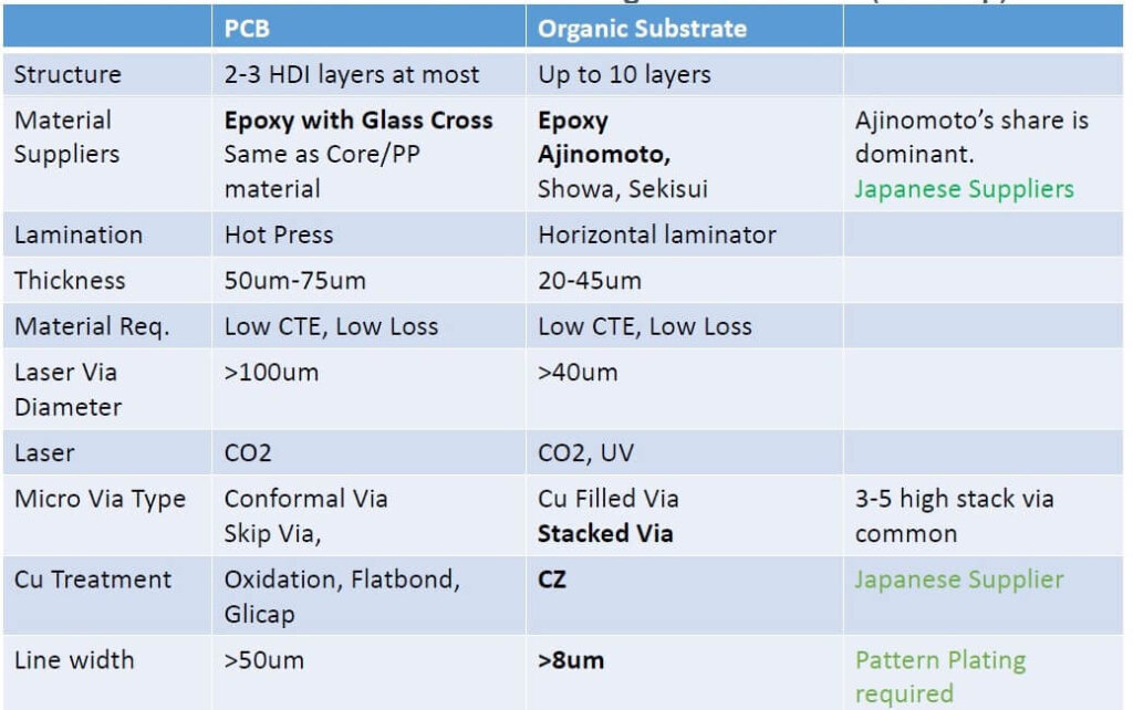
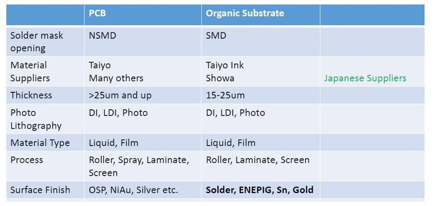
The Difference Between HDBU and HDI
Even more interesting is their comparison of the differences between HDBU substrates and high-density interconnect (HDI) boards (Figures 6-9).

Kyocera listed the following challenges for the production of HDBU substrates in the US mainland.
Supply Chain
- Most of the materials are imported from Japan. Possible to import for prototyping
- Longer material lead time
- Material transportation method: Refrigerated or frozen
- Higher material cost
- Importing material restriction, TSCA, etc
Equipment
- Key equipment for buildup processes is made in Japan
- Can use some PCB processes for the core and backend.
Clean Rooms
- Need Class 1K, 10K clean room for most processes for yield improvement.
Staffing
- Challenging to find experienced engineers and workers in organic substrates
- Salary and wages in the US are much higher than in Asia
- Environment and Safety
- Water supply, wastewater treatment
Even with the aforementioned obstacles, Kyocera indicated that they understood the importance of onshoring organic substrates to the US market, especially the military DoD market, and have been seriously reviewing the possibility of onshoring their HDBU technology to their current San Diego ceramic facility.
For all the latest in advanced packaging stay linked to IFTE……………………………………….


