
IMAPS DPC 2022
This year’s IMAPS Device Packaging Conference (DPC) was live once again, though most of the live attendees were from the US and far fewer were from Europe and Asia than usual. The unique aspect of this year’s meeting was certainly the Global Business Council session (GBC) which focused on the DoD SHIP contracts and the reshoring effort.
Over the next few blogs, we’ll take a look at some of the interesting presentations at the conference.
AMD Advanced Packaging
You may recall Raja Swaminathan was the AMD senior fellow speaker at the IEEE 3DIC Conference earlier this year. At the IMAPS DPC, his plenary presentation was entitled “Advanced Packaging: Enabling Moore’s Law’s next frontier through Heterogeneous Integration.”
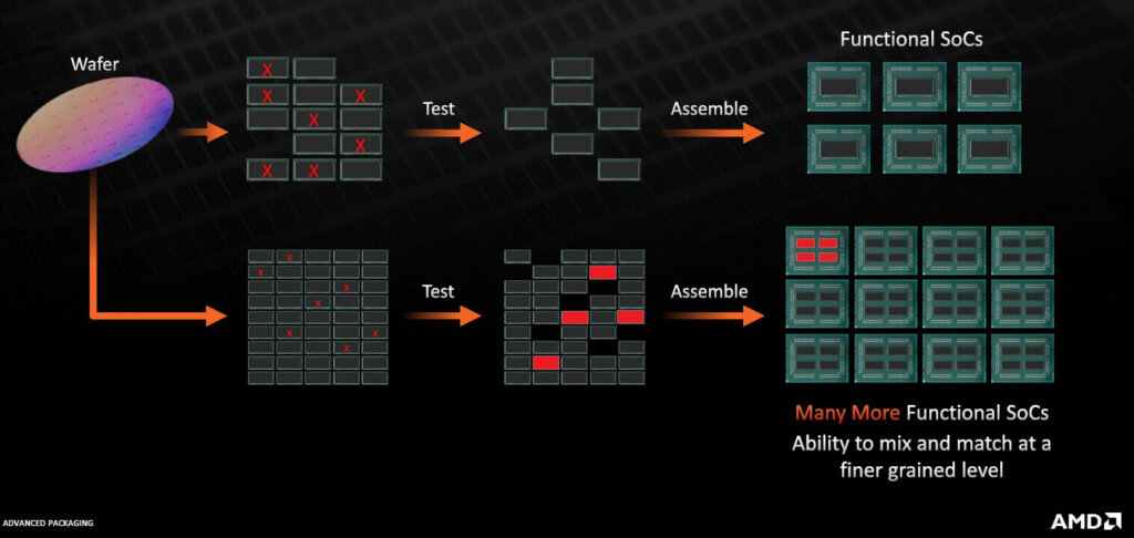
His first point about chiplets was that you end up with many more final devices because the yield of the smaller chiplets is significantly higher than large systems on chip (SoCs) (Figure 1).
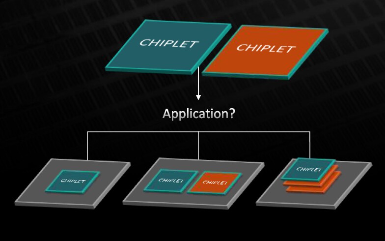
The goal is to build tailored products for specific markets by mixing and matching chiplet types. They can now specialize a domain-specific chiplet and include more or fewer of them for a specific product (Figure 2).
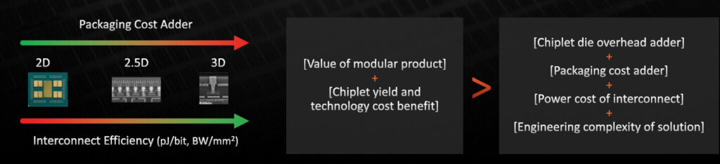
Chiplet architecture selection involves balancing a complex equation as shown in Figure 3, and these parameters must be carefully analyzed to determine whether chiplet use will be economically viable.
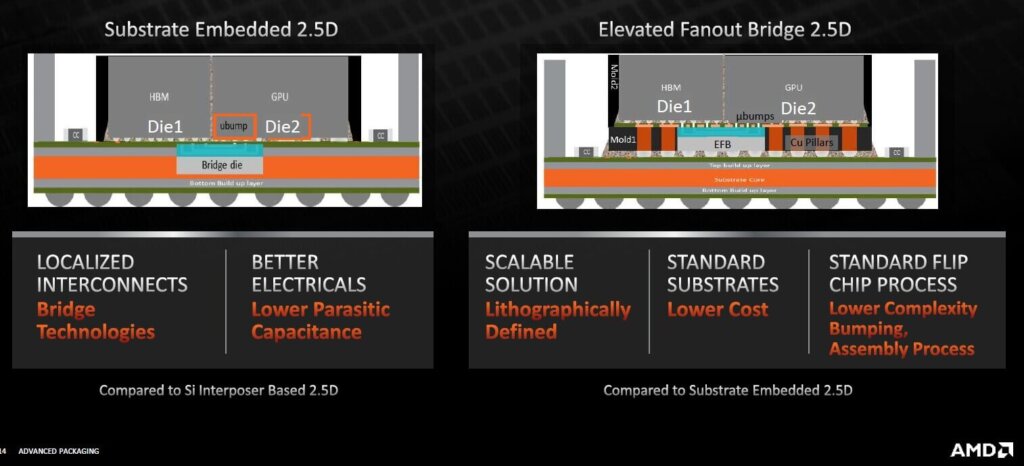
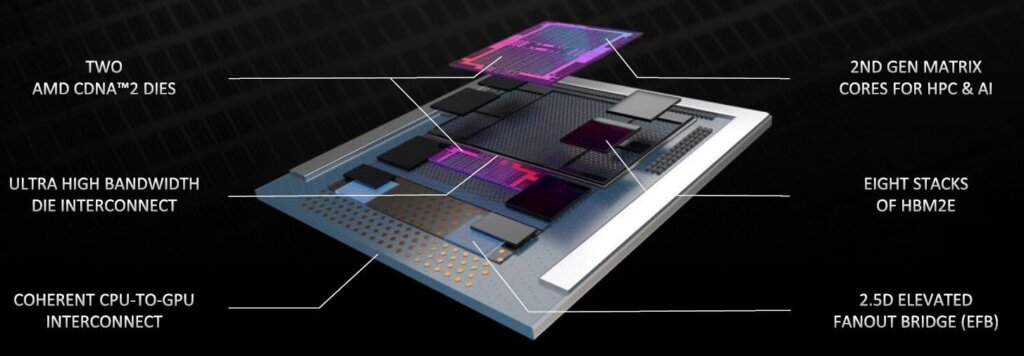
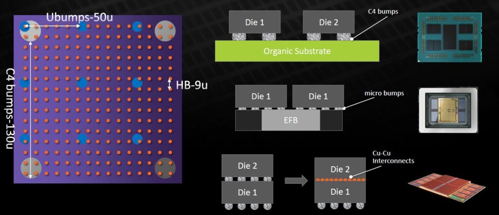
Then Raja showed this interesting comparison of an Intel-type embedded bridge technology compared to elevated fan out bridge technology that they are using for their MI200 series modules (Figures and 5).
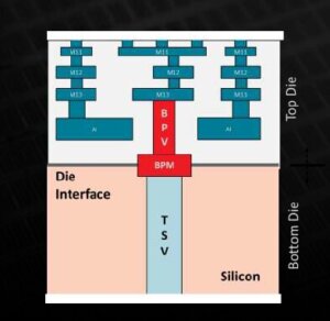
Raja then described the use of AMDs 3D V-cache, which uses TSMC SoIC hybrid bonding technology (Figure 5).
- Cu-Cu hybrid bonding using bond pad metal (BPM) pads
- Bond pad via connects BPM to M13
- 9um min TSV/hybrid bond pitch

Lastly, Raja commented on the future of 3D stacking showing how it will migrate down to ever smaller dimensions and ever-smaller partitioning.
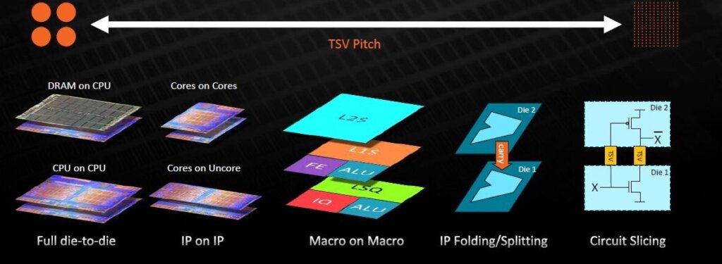
In a subsequent paper, “Heterogeneous Integration with 3D Packaging”, given in the regular sessions, Rahul Agarwal of AMD detailed how the interconnect technology has moved from stud bumping to micro bumping to hybrid bonding (Figure 8), and gave further detail on the AMD use of the TSMC SoIC hybrid bonding process.
They report the Cu-CU hybrid bonded interface is “ultra-robust”, having successfully passed several JEDEC reliability tests. They report that the technology has been “fully qualified”. This technology will be used in the 3rd gen EPYC server CPU and the RYZEN 7 gaming CPU.
For all the latest in Advanced packaging stay linked to IFTLE………….


