
This week we’re looking at some packaging presentations from the 2021 IMAPS Device Packaging Workshop. The focus is on Nepes mPoP and Sumotomo Bakelite EMC.
Nepes – Fan Out mPoP
BC Kim described Nepes M-series fan-out package mPoP. mPoP is a stackable package-on-package structure used to provide an integrated solution for application processors plus memory devices as shown in Figure 1. He explained that mPop is based on Deca’s M-series technology, which Nepes licenses. Connection from the front side of the application processor to the memory is done using large copper posts. The mPoP has one layer of RDL (redistribution layer) and 8µm line/space (L/S). Kim says the company is commercializing the technology and is ready for customer engagement.
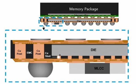
Figure 2 shows the mPoP process flow. These are being made on 300mm wafers and 600 mm2 glass panels.
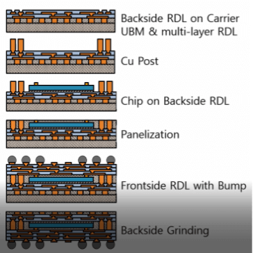
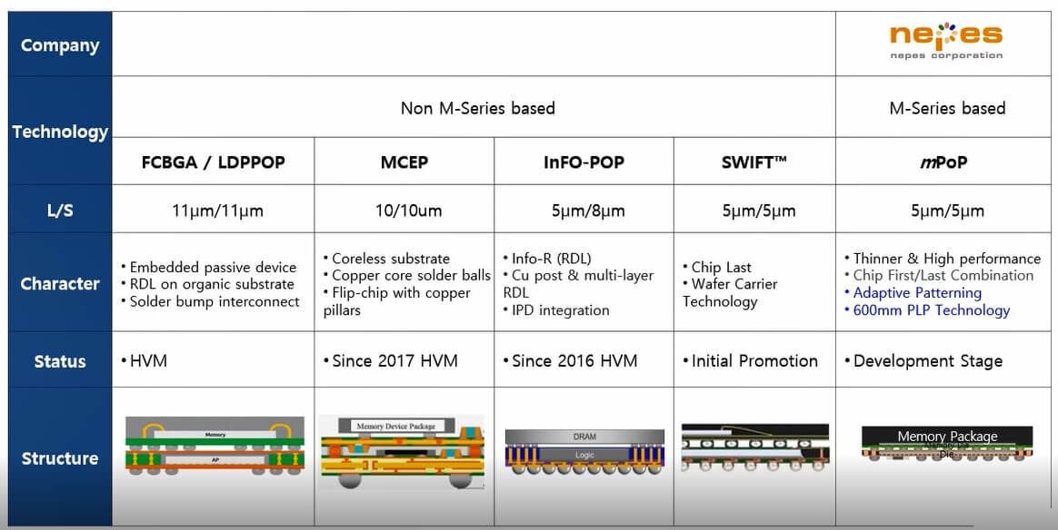
Table 1 compares Nepes’ solution to other high-density PoP solutions (5um L/S)
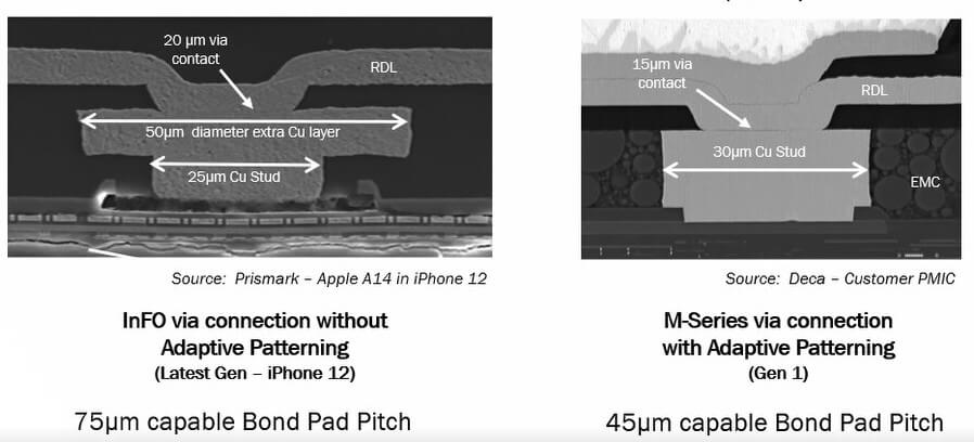
Kim says Nepes has the capability to create smaller features than TSMC’s integrated fan-out (InFO) technology. He reports that the extra 50µm Cu layer is necessary for the InFO structure because of alignment issues. Deca’s M-series technology makes it possible for them to use adaptive patterning so they can align the smaller features (Figure 3).
In addition, Kim says Nepes can move to an ultra-high-density solution (2µm L/S and 5µm vias) by moving to Gen-2 adaptive patterning and laser direct imaging, which should reduce the current 4µm die pad pitch down to 20µm.
He said he thinks that their 600mm panel-level packaging (PLP) solution gives them a cost advantage over other options.
Sumitomo Bakelite – EMC for fan-out WLP
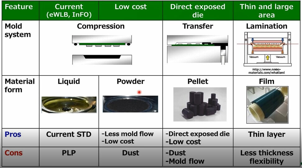
Masahiro Iwai of Sumitomo Bakelite (SB) discussed the latest EMC (epoxy mold compound) technologies for fan-out WLP. Molding technology options are shown in Figure 4.

Iwai claims that the powder (granule) type EMC has adhesion and toughness advantages over liquid mold compounds and the liquid materials cannot be used on PLP. He said dust issues have been resolved by tool vendors such as Towa and better particle size control gives them better flow performance.
One of the keys for FO-WLP manufacture is warpage control. Iwai says SB has found a “stress index” parameter (E x CTE) correlates with warpage. = modulus) Adding a low-stress additive (LSA) can substantially reduce the stress index value and thus the overall wafer warpage as shown in Figure 5. The LSA must be adjusted to match the RDL dielectric to maximize adhesion.
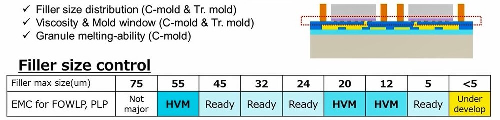
Control of EMC particle size is important to allow flow and complete fill in tight dimensions. Currently, 5µm particle size filler is being used with smaller particles under research.
For all the latest in Adv Pkging stay linked to IFTLE……………………………………………………..


