

The IEEE International Solid-State Circuits Conference, – ISSCC 2021 – took place in late February. As we have suspected for some time, these formerly front-end conferences are more and more focusing on packaging and the performance advances you get from new packaging architectures.
Let’s first take a look at what TSMC Chairman Mark Liu had to say in his ISSCC 2021 plenary talk of “Unleashing the future of Innovation”.
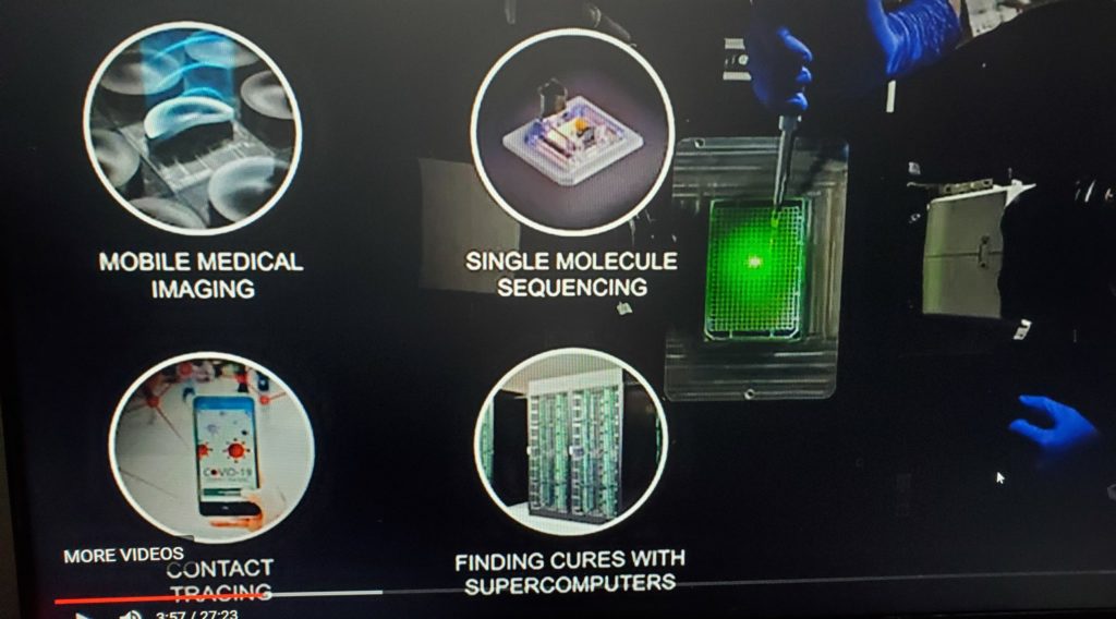
The semiconductor industry is a foundational technology and is more important than ever. As an example, he then stressed the impact that the electronics industry has had on fighting the pandemic. Some of these impact areas are shown in Figure 1. Today technology is fully integrated into our lives and semiconductor innovation is at the heart of technological innovations.
Advanced Technology Nodes Offer the Highest Speeds and the Highest Energy Efficiency
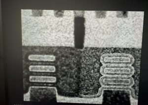
Liu notes that industry and academia have been working closely together to develop new transistor structures, new materials and new system architectures, and 3D integration so that we can sustain advancements beyond 3nm. Going beyond the FinFET, nanosheet transistors may offer additional performance and power efficiency (Figure 2).
Because of intrinsic scaling metrics, gate pitch and metal line pitch no longer reflect the actual logic density of a technology [for further discussions about this read IFTLE 462 “If not nodes then what?]
TSMC is also highlighting innovations beyond the chip level as shown in Figure 3.
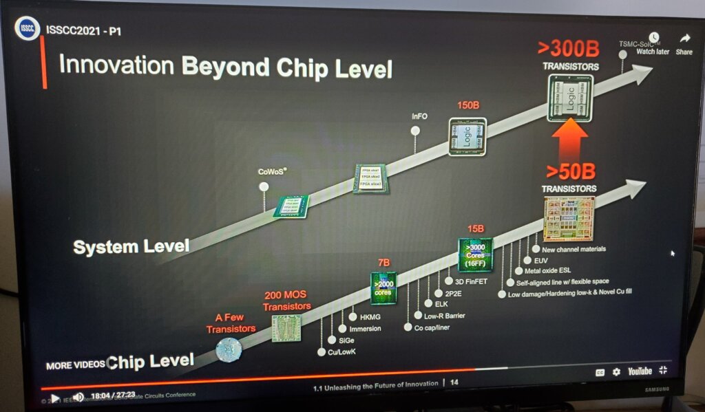
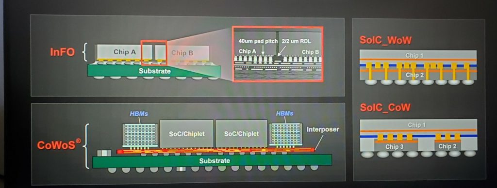
Liu highlighted how TSMC’s Integrated Fan-out (InFO,) chip-on-wafer-on-substrate (CoWoS) and system-on-integrated-circuit (SoIC) technologies have opened up ways to increase the transistor count in these packages to over 300B. The combination of these technologies is now known as TSMC 3DFabric (Figure 4). Liu emphasized that SoC is no longer the only optimal system. Systems with several chips packaged together and chiplet based architectures will play an increasingly important role.
TSMC is calling splitting out chiplets of a specific function and optimizing production as its “domain-specific technology approach”. He claims that recent advances in system integration like their 3D fabric technologies have made it economical to partition a system, optimize and reassemble. The company also sees major advancement coming from its SoIC bonding technology showing a 12 active chips layer (total of 600m thick) chip stack using low-temperature bonding.

Liu claims that chip-to-chip interconnect density has the potential to increase another four orders of magnitude using SoIC.
In conclusion, system integration in a package is emerging as a complimentary system-level booster to transistor count, performance, and energy efficiency. TSMC sees the future as system integration. IFTLE once again will remind you that MCMs, SiP, heterogeneous integration, chiplet assembly are basically all saying the same thing, i.e. using modularization to achieve the next generation of technological advancements.
Many of us have been waiting for decades for packaging to become King and it is now happening!
For the latest in Advanced Packaging stay linked to IFTLE……………………


