
 The November Issue of Chip Scale Review contains some interesting advanced packaging information that is worthy of sharing in IFTLE: the cover story on fluxless µbumping by ball placement, and Yole’s look ahead at stacking technologies.
Fluxless µBumping by Ball Placement
CC Dong from Air Products examined fluxless micro ball placement bumping technology.
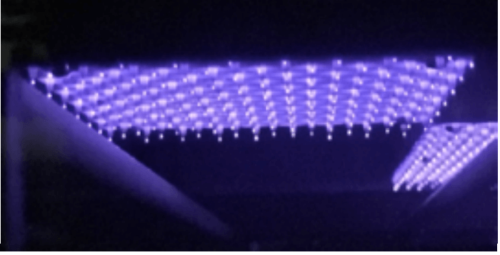
Bumps on a flip-chip (FC) package are typically in the range of 100 – 200µm in height. Micro bumping for high-density packages can have pitches as low as 55µm. Wafer-level packages (WLP) are normally in the range of 250 – 500µm in height. Solder deposition can be done by paste printing, plating or ball placement. Paste printing is a low-cost approach, but cannot be used for fine-pitch micro bumps. Plating is currently the method of choice for most bumping but is more expensive. Ball placement has now been developed over the full range of 50 to 500µm solder balls.
The first step in ball placement is to deposit an organic flux on the wafer pad areas. During reflux, the oxide on the surface of the solder balls and pads is cleaned and then the solder is melted. Post reflow, a cleaning step is required to remove flux residues. For micro-bumps, the flux residue can become wrapped between the solder balls.
Air Products is developing a fluxless µ-bumping Hydrogen-based (H2) technology, using non-flammable 4% H2 /nitrogen as the reducing agent technology, to replace the fluxing and cleaning steps. Air Products has developed a “locating agent” to replace the flux in terms of holding the solder balls in place.
The company has also developed an “electron attachment” (EA) device, which is mounted inside the furnace and emits low energy electrons to activate the hydrogen. Such furnaces are reportedly now being manufactured commercially.
By applying the EA-activated hydrogen in a forming gas environment, oxides can be eliminated from the solder and copper pad surfaces reportedly resulting in 100% ball attachment with good solder wetting. The “locating agent” is reportedly decomposed in the EA H2 atmosphere without leaving any residue reportedly eliminating the need for a post reflow clean. [ Note: IFTLE would like to see more data before accepting this claim] Without the EA, the solder wetting is reportedly poor and the decomposition of the locating agent is reportedly incomplete.
Latest on Stacking Technologies
Shoo, Yole Dévéloppement, looked at “Stacking Technologies: The Road Ahead”
High-performance computing (HPC), AI, data center computing, and big data analysis, etc. require low latency, high speed, and low power consumption. TSV stacking, hybrid bonding, and chiplet disintegration technologies are being examined as potential solutions to these problems. Cost performance and footprint are three of the key parameters that customers are looking at when deciding between these solutions.

Yole sees foundries, IDMs, OSATs, and IP companies all competing to get their share of the stacking pie. In the 3D stacked memory market, the battle is among the big three of Samsung, SK Hynix, and Micron. They report that Samsung has a 70% market share followed by Hynix. Micron currently has no HVM of HBM memory stacks so it has fallen significantly behind.
Foundries like TSMC, UMC, and GF dominate the TSV stacked technology market because of their ability to manufacture silicon interposers in house. Samsung, Intel, and TSMC have developed high-density stacking technologies with and without TSVs. For the TSV-less high-density stacking technologies foundries, IDMs, OSATS, and substrate manufacturers are all competing with the substrate companies like Unimicron, Shinko and Fujitsu Interconnect still in R&D.
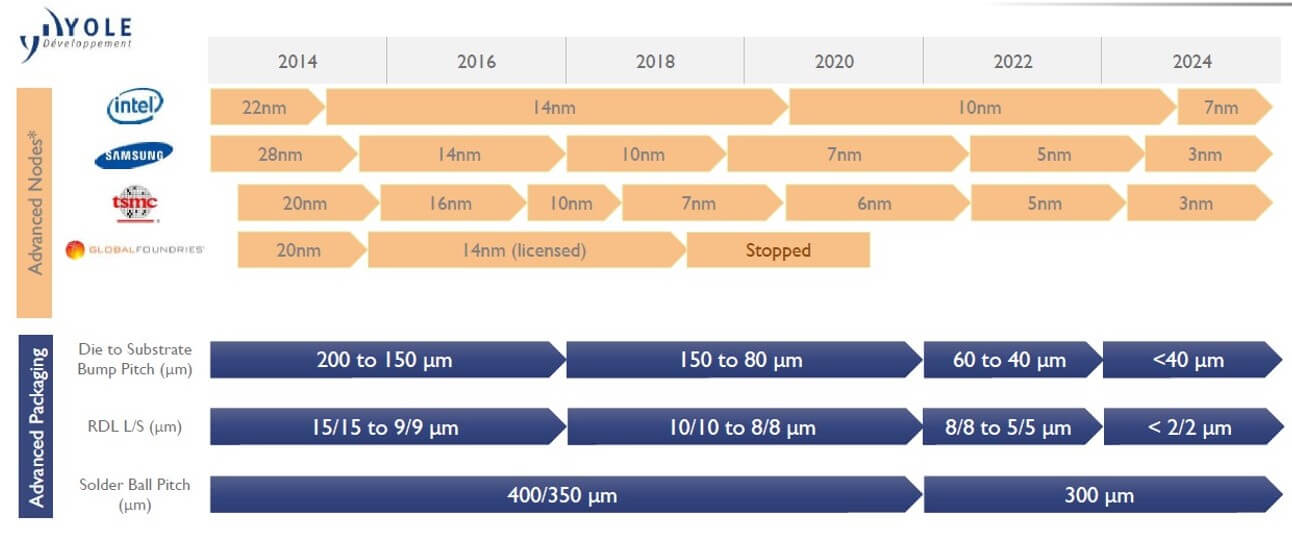
The following two figures summarizing what they see happening in the space.
For all the latest in Advanced Packaging stay linked to IFTLE…………………….


