

The special Tuesday session at ECTC 2018 took a look at new methods and applications for assembly technology to accommodate the needs of heterogeneous integration at the system level. The session was chaired by Florian Herrault, HRL Laboratories, and featured Jeff Demmin, DARPA; Stefan Behler, Besi; Matthew Meitl, X-celeprint; Doris Tang, PlayNitride; and Val Marinov, Uniquarta. Presentations offered the latest advancements in assembly technologies for chip packaging, microLED displays, and ultra-thin chip placement for flexible electronic applications, respectively. This post focuses on the two that impacts interposer and 3D integration the most.
What do DAHI, MECA, CHIPS and ERI have in common?
DARPA. If awards were handed out for the presentations with the most acronyms, DARPA’s Jeff Demmin would be a big winner. Demmin kicked off the special session:
Demmin updated us on DARPA’s Diverse Accessible Heterogeneous Integration (DAHI) program, which is developing transistor-scale HI processes to integrate compound semiconductors and other mixed technologies with high-density CMOS technology.
This marked the second time I heard reference to the part of Moore’s Law that’s been summarily ignored up until now: The second paragraph where it INCLUDES heterogenous integration. “At some point, it will be cheaper to build things separately and put them together,” explained Demmin. “That’s not usually what you read in the headlines about Moore’s Law.”
He highlighted Herrault’s work on HRL’s award-winning metal embedded chip assembly (MECA) process that enables HI. MECA is important to DARPA’s Common Heterogeneous Integration and IP Reuse Strategies (CHIPS) program, which is an integration platform targeting standards and modularity.
“CHIPS will develop design tools, integration standards, and IP blocks required to demonstrate modular electronics systems that can leverage the best of the DoD and commercial design and technology,” noted Demmin.
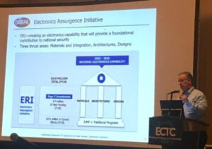
Demmin wrapped up his talk by announcing a summit to support CHIPS new Electronics Resurgence Initiative (ERI), which focus on three thrust areas – materials and integration, architectures, and designs – to create an electronics capability that provides “a foundational contribution to national security.” The summit takes place July 23-25, 2018 in San Francisco.
Hybrid Bonding: Winner Winner, Chicken Dinner!
Thermocompression bonding, take notice: your days are numbered. Hybrid bonding, already established in sub-micron accuracy wafer-to-wafer (W2W) bonded SOCs, is about to replace you for die-to-wafer (D2W) bonded 2.5D and 3D SiCs. Furthermore, hybrid D2W bonding will compete with hybrid W2W bonding for 3D SOC production in near future.
These two radical scenarios can be concluded from the work of Besi’s Hugo Pristauz, (known to 3D inCites readers for his disruptive ideas and occasional f-bombs), which was presented by his colleague and co-author, Stefan Behler, during the Assembly Frontiers session.
Behler explained the advantages of hybrid bonding over TCB; most significantly the ability to bond at room temperature to enable smaller bump pitches in the micrometer range. The authors agree with Subu Iyer from UCLA that the optimal bump pitch for 2.5D chiplet assembly is 2-10µm, which can’t be done with TCB.

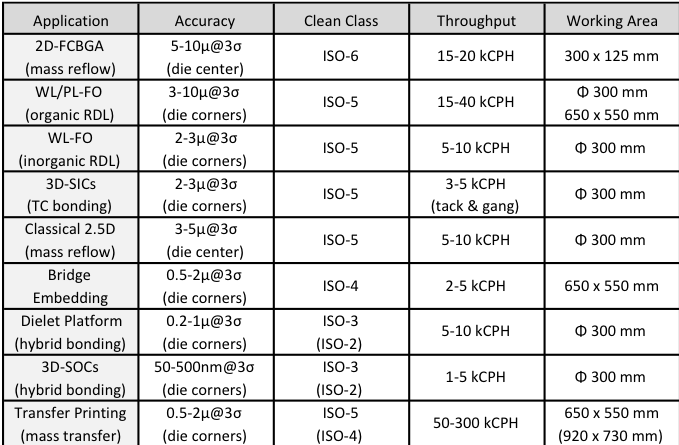
The table below explains the placement accuracy, clean class and throughput requirements for different heterogeneous integration approaches by application.
According to Pristauz, the only justification for D2W TCB right now is the lack of available D2W equipment designed to meet the needs of productive hybrid bonding; namely class 1 cleanroom standards in combination with high throughput.
In addition, the implementation of productive hybrid bonders with sub-micron placement accuracy of 200nm@3σ at each corner (with a roadmap driving down to 50nm@3σ) will open the doors for 2.5D chiplet platforms and enable D2W bonding for 3D SOC applications.
These tools targeting high productivity are currently in development, and once available will not only make 3D SOC D2W hybrid bonding possible, moreover will increase productivity for 3D SIC assembly, namely high bandwidth memory (HBM), eliminating the complicated thermal process to make stacking of 32 layers possible with the additional benefit of gap reduction between stacked dies.
If Pristauz’ predictions are going to come true, we are facing a game changer, which could mean the end of TCB for 3D memory production in 3-5 years. ~ FvT


