
There’s fact, and there’s perception. The messages people carry away from conferences are not only influenced by what they hear from the speakers, but also from the conversations they have with their colleagues. This post contains a little of both.
At IMAPS Device Packaging Conference in March, Yole Developpement analyst, Emilie Joliet announced to the industry that at long last, 3D integration is taking off for real and that 2018 will be the “golden year” for volume production increase of both 3D through silicon vias (TSVs) and 2.5D platforms driven by high-performance computing (HPC), artificial intelligence (AI), and deep learning.
Last week, during his luncheon keynote at ECTC 2018 about what’s needed to enable these rapidly growing markets by 2022, Broadcom’s Boon Chye Ooi confirmed it: AI, autonomous vehicles, and wearable devices need 5G. And word on the street is, 5G needs 2.5D and 3D.
Ooi predicted that during peak hours, IP traffic will be 3-5X more than we have now in 2018, and that wireless and mobile devices will account for 63% of total IP traffic.
“It (5G) is going to come sooner than we think,” he said. “The US may not be there first in this area, as the infrastructure isn’t there yet.” Nevertheless, systems and devices need to be ready, and IC packaging technologies will be a key enabler.
Consider the following: According to Ooi, data rate challenges can be solved by 2.5D integration of, for example, a custom ASIC surrounded by 8 high bandwidth memory (HBM) chips. But these power-hungry 900-watt devices have to dissipate heat on the package. Additionally, with Moore’s law driving chips to 7nm, 5nm, and even 3nm, packaging that becomes a challenge. Enabling AI, said Ooi, requires 4 Gbps HBM and 4nm interposers. 3D could be the solution. GLOBALFOUNDRIES gets it: they have designed a 3D SRAM stacked on a microcontroller for machine learning applications.
Fan-out was a Sold-out Show
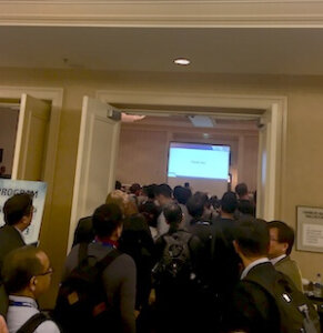
As has been the case for the past few years, the fan-out (FO) sessions – both panel-level and wafer-level, were not only standing-room-only, they spilled out into the hallways.
Interest in FO is at its peak not only because of the acclaim it has received from winning star placement in the Apple A7 microprocessor chips for its iPhone, but because of all the other components in other mobile devices it provides solutions for in both low-density and high-density formats.
Despite the large draw, however, I’m told the presentations were not revealing anything new or earth-shattering. Most were focused on incremental improvements in optimizing processes for RDL to reduce line/space for achieving high-density fan-out HDFO. Others addressed the second hottest topic to FO itself: panel-level packaging (PLP).

The buzz from behind the scenes explained why. (For some reason, people like to tell me stuff – but then they don’t want me to quote them) So without naming names, here’s some food for thought from people who know a lot more about this than I do:
While the major outsourced semiconductor assembly and test service providers (OSATs) have invested in developing technologies to optimize HDFO platforms, in reality, TSMC might be the only game in town. My sources predict that because of its ability to control the damascene processes that are critical for RDL, TSMC will likely own this space. The OSATS will need to either install RDL lines or source it from a foundry. But why would TSMC want to provide that when they can do the whole thing themselves? Think about it: when is the last time we heard anything about Xilinx’ silicon-less integrated technology (SLIT) and Amkor’s silicon-less integrated module (SLIM)? Time will tell how this plays out.
Now, most of the OSATs are focusing efforts now on FO panel-level processing for their low-density versions already in the mainstream, as a way to lower cost, enable larger die sizes, and extend the technology into – you guessed it – the third dimension.
So Is 3D making a Comeback?
Some say yes, absolutely. Others say it never really went away. People got bored waiting for it to hit the big time and shifted focus to the next big thing: FO. So, it’s really more that 3D’s time has finally come. What changed? After a few years of disillusionment, 3D is becoming hot again, this time as 3D systems integration. This photo of a slide snapped during Ooi’s keynote presentation says it all: It’s turning out to be a cheaper route than SoC as we reach smaller nodes – 7nm, 5nm, etc.
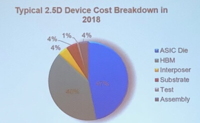
Why? SoCs are expensive. Partitioning into IP blocks (known as chiplets or dielets) and going vertical reportedly saves 40% in silicon costs. Whereas a few years ago, it was thought that TSV and interposer expenses were making 3D cost prohibitive for anything but high-performance computing applications, it’s now proving that only 4% of the cost is in the interposers. Go figure.
Stay tuned for more from ECTC. ~ FvT

