
Despite a valiant effort by the ECTC committee to integrate design topics into this year’s agenda, the number of empty seats spoke volumes: Including two plenary sessions on design-focused topics was one thing; getting packaging and process engineers to attend was quite another. While I attended IC Package Co-Design for HI Systems and AI and Its Impact on System Design, I have to admit, I found the presentations hard to understand because I simply don’t speak design. (But I’m pretty sure I’m not the only one.) What follows is my attempt to decipher the over-arching messages.
IC Package Co-Design for HI Systems
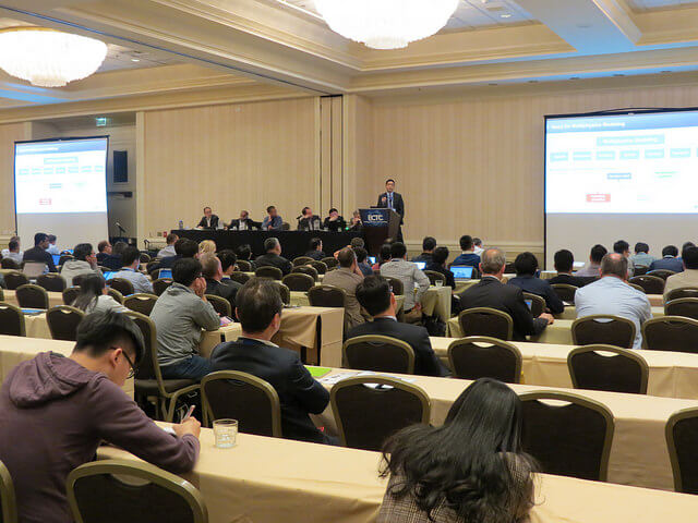
Co-chaired by IEEE-EPS president Avi Bar-Cohen and Chris Bailey, University of Greenwich, panelists were asked about state of the art for co-design, what are the challenges, solutions, and remaining gaps. Panelists hailed form varies technology areas and provided perspective based on respective core competencies. Harrison Chang, ASE represented the OSATs. John Parry, Mentor Graphics, represented EDA vendors. Yong Liu, On Semiconductor, represented power semiconductors. Xue Fan, Lamar University; Madhaven Swaminathan; and Andrew Kahng, UC San Diego; provided the research expertise.
Essentially, designing systems that can integrate all the disparate components, materials, each with different physical properties and requirements requires understanding the interaction between the chip, package, and board. All contribute different stresses that can contribute to failures.
Some key take-a-ways:
- HI is not just about advanced packaging – it will encompass power electronics, flexible electronics, LEDs, semiconductors, photonics, and more.
- Tools currently exist, but there are some significant gaps.
- A single modeling approach is not enough. It requires multi-physics modeling.
- A free, open-source software ecosystem could address HI co-design needs.
Technically, thermal co-design is feasible today, noted Parry. The main remaining challenge is awareness-raising. The need to do thermal design is not often recognized until it’s too late. After 30 years, people are still using hand-calculation rate of speed system design. The IEEE HIR roadmap will change that.
Offering the perspective from the power semiconductor segment, Liu said what’s needed is a “differentiating and cost-effective co-design infrastructure that goes beyond the current platform of exploration, simulation, and design verification, methodology and development sharing. It needs to provide multi-scale and multi-physics design challenges, as well as multi-step process variation probability. Liu added that a co-design ecosystem and virtual prototyping is coming soon for power electronics.
Kahng pointed out that while co-design tools exist for HI, we come up short with pathfinding and design space exploration tools. “We are preoccupied with checking things. There’s not much being done about optimization,” he said. The most significant pain point is that existing tools live in three different worlds, leaving many cross-domain tool gaps. We need something that connects the three worlds of die, package, and board.
Are data centers the new Moore’s Law?
In terms of sheer computing power, yes, noted Microsoft’s Andrew Putnam during the plenary session on AI and its impact on system design. Predicting that AI will be a $100B industry in “a handful of years,” he said that cloud growth is exponential: In the past five years its grown 100% year over year. Deep Learning (DL) is pushing high-performance computing (HPC) from specialized clusters into the general-purpose fleet, noted Putnam.
Kailash Gopalakrishnan, IBM talked about the training aspects of AI/Deep Learning applications and algorithms. He said the slowing of Moore’s law has enabled companies to focus on building new SoC architectures for AI and deep learning.
Memory bandwidth is the bottleneck for AI/machine learning. Companies are exploring ways to solve this. Microsoft puts neural networks in on-chip DRAM memory to get terabytes of memory bandwidth out of an FPGA. Others, like Broadcom, are combining ASICS with HBM.

In addition to memory, AI applications are power hungry. According to GLOBALFOUNDRIES Igor Arsovski, electronics for AI are 50K more power hungry than the human brain. System architectures need to be more energy efficient.
“Memory capacity and energy access are critical for AI application,” said Arsovski. “We would like to see the industry focus more on memory to enable the AI roadmap.” For their part, GLOBALFOUNDRIES is working on ASICs for AI and 3D SRAM memory, because 3D stacking enables multiple node memory density scaling. The goal, he says is to use 3D integration to minimize the power need to get in and out of memory, but we are still far off.
Offering Samsung’s perspective, Dan Oh commented that design and process engineers don’t talk to each other (note my earlier point). Design engineers use minimum ground rules. Process engineers spin designs repeatedly.
It’s important to make sure designs are manufacturable, he explained. Machine learning can be used to train models. “Engineers are thinkers. Computers are the doers. Machine learning is the enabler,” he said.
Oh touted Samsung’s GDDR6, the company’s recent advancement in DRAM, as an ideal replacement for high bandwidth memory (HBM) for deep learning inference servers, HPC, the blockchain, and automotive applications. Additionally, he said low-latency SRAM devices may be a good solution for inference.
And that’s all I’ve got. I invite anyone who understood more to comment here. ~ FvT


