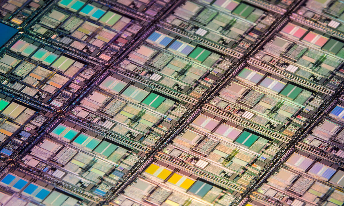
![Rama_Alapati_Color_Jun2016[1] copy](https://3dincites-imaps.nyc3.digitaloceanspaces.com/wp-content/uploads/20240828181856/Rama_Alapati_Color_Jun20161-copy-1.jpg) In the fourth installment of the series “Convergence on the Big Five,” we compared conventional SiP with advanced system-in-package (SiP), which is focused on laminate-based approaches, and is available and in production today. Advanced SiP packaging has been a game changer in addressing system-level integration and providing the lowest form factor at cost and performance points that address market needs in RF, solid state drives, automotive, IoT, and power segments. In this fifth and final installment, we continue the conversation with a look forward into wafer-based advanced SiP, and how its promise will drive the industry into next-generation devices to support the connected world of the future.
In the fourth installment of the series “Convergence on the Big Five,” we compared conventional SiP with advanced system-in-package (SiP), which is focused on laminate-based approaches, and is available and in production today. Advanced SiP packaging has been a game changer in addressing system-level integration and providing the lowest form factor at cost and performance points that address market needs in RF, solid state drives, automotive, IoT, and power segments. In this fifth and final installment, we continue the conversation with a look forward into wafer-based advanced SiP, and how its promise will drive the industry into next-generation devices to support the connected world of the future.
Like laminate-based advanced SiP, wafer-based advanced SiP allows for the integration of complex and disparate technologies, but meets the higher performance; bandwidth, form factor and density requirements in HPC, IoT, mobility, and automotive segments. In addition to integrating basic microprocessors, sensing elements (MEMS or image sensors), RF dies, and power management ICs, wafer-based advanced SIP is also used to integrate memory (HBM, HMC etc.), ASIC devices, and high-performance processors, such as graphics processor units (GPUs) and FPGAs.
Wafer-based Advanced SiP
In considering the “Big Five”, which Amkor considers to be: low-cost flip chip, wafer-level chip-scale packages (WLCSP), MEMS and sensor packaging, and laminate-based advanced SiP, the final segment, wafer-based SiP, is the technology that serves the widest scope of applications.
Wafer-based advanced SiP is currently targeted for high-end devices and is still in the early phases of introduction to the industry. It effectively addresses system-scaling needs and can help offset or delay the need for next-generation Si node based products. Its initial market entry points are high-performance computing (HPC), memory, and high-end mobility. Over time, however, we believe more devices will take advantage of wafer-based SiP technology to enable extreme form factor reductions and increased product performance at lower power.
While laminate-based SiP leverages the existing die scale infrastructure, wafer-based processes differ significantly from laminate-based processes and require investment in wafer processing tooling. Wafer-based SiP replaces and/or complements the laminate substrate, providing redistribution layer (RDL) line/space (l/s) features down to 1µm x 1µm. Wafer-based SiP RDL can scale to Fab BEoL like dimensions, whereas traditional laminate-based advanced SiPs are currently limited to 10µm x 10µm l/s. Therefore, wafer-based SiP systems provide the best-in-class (BiC) scaling capability while at the same time having the ability to scale to fab-like dimensions.
As my Amkor colleague, Ron Huemoeller, has noted in his presentations at various industry forums, the semiconductor industry requires much higher levels of integration in a significantly reduced form factor where multiple die technology must exist within the same package footprint. Wafer-based advanced SiP technology enables this integration. At Amkor, we are leveraging our significant knowledge and capability in this area to provide cutting-edge package technologies, such as SWIFT™ and SLIM™. The package and board-level reliability results we have recently attained for our SWIFT package technology affirm that our wafer-based advanced SiP products are ready for sampling.
There are increased costs associated with wafer-based SiP due to the complexity of the products produced. One of the contributors to the increased costs compared to laminate-based advanced SiP is the CapEx required to build a platform for wafer-based processes in Class 1 or Class 10 cleanrooms. Fab like infrastructure and additional toolsets including those used for traditional front-end processes such as physical and chemical vapor deposition tools, chemical mechanical planarization tools, and temporary bond/debond systems, contribute to the increased upfront costs required to enable wafer-based SiP platforms. As the tools and factories depreciate, the manufacturing costs of wafer-based advanced SiP will be reduced, enabling a wider set of applications to take advantage of the form factor reduction and significant product performance increase.

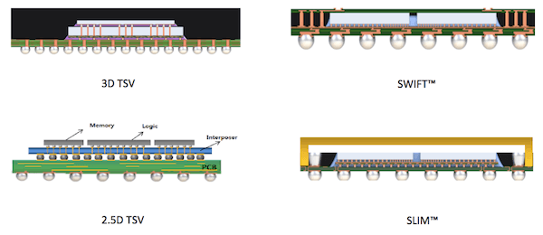
Package configurations in the wafer-based advanced SiP family include high-density fan-out wafer-level packages such as Amkor’s SWIFT and SLIM product lines. These configurations use a “die last” approach that minimizes the yield loss risk prevalent in the complex die first WLFO packages. SWIFT is expected to ramp to production in the next few quarters and become a predominant driver of wafer-based advanced SiP products. The SLIM and SWIFT small body sizes have passed CPI qualifications, with large body sizes in development. Also on Amkor’s wafer-based advanced SiP roadmap are 2.5D interposer and 3D IC stacks. 2.5D TSV is available today, having been qualified since 2013. Amkor is working with ecosystem partners to not only provide a seamless supply chain and qualified Si portfolio but also to enable co-design by providing design kits for each of the wafer-based SiP platforms.
Conclusion
In summary, the mobility market is driving form factor reduction and high density interconnect for multi-die integration. In the HPC, networking, deep learning, and GPU applications, wafer-based advanced SiPs address the power, memory bandwidth and latency issues of new devices coming to the market in the next couple of years. 2.5D, 3D, SLIM and SWIFT technologies can potentially help OEMs and fabless companies delay migration to the next node by enabling system-scaling approaches through wafer-based SiP.
Wafer-based advanced SiP rounds out Amkor’s Big Five portfolio, allowing continued innovative choices that will help achieve the best performance, form factor and value-to-cost ratio for any application. ~ R. Alapati