


“The sum is greater than the whole of its parts.” ~ Aristotle (and Bill Chen)
While the technology tracks offered the latest developments in interposer and 3D IC processes, fan-out, wafer-level packaging, flip chip, MEMs, sensors and more, System-in-package (SiP) was the big story of the 2016 MAPS Device Packaging Conference, which was held March 15-17, 2016 in Fountain Hills, AZ. Why? Because SiP is the sum of all the advanced packaging parts, including interposer and 3D interconnects, and truly provides the value-add that advanced packaging now brings to semiconductor manufacturing.
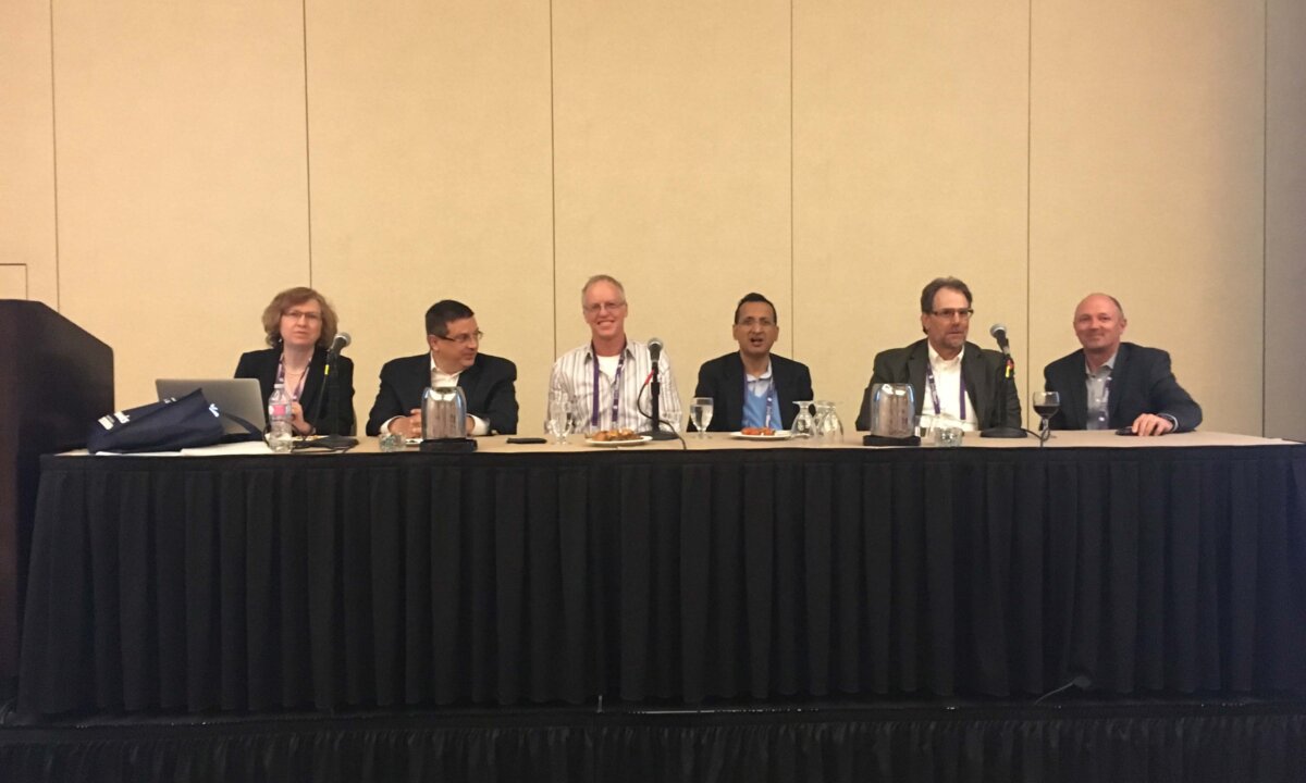
There are many definitions of SiP, as we learned from the panelists on Tuesday evening’s SiP Panel, from Rozalia Beica, in her presentation during the Global Business Council, and from Bill Chen in his keynote on Fan-Out SiP:
• Rich Rice, ASE: SiP module is a package or module that contains a functional electronic system or subsystem that is integrated and miniaturized through IC assembly technologies.
• Lee Smith, UTAC: SiP involves heterogeneous integration of diverse functional parts into a standard package format (BGA, leadless, leadframe). It can include passives components and mixed assembly technologies.
• Rozalia Beica, Yole Développement: A SiP is two or more components with different functionalities packaged as a system or subsystem.
• Bob Lanzone, Amkor: we define advanced SiPs as multi-component, multi function products in an IC package. They require high-precision assembly technologies, which leverage Amkor’s strengths.
• Bill Chen, ASE: Heterogeneous Integration refers to the integration of separately manufactured components into a higher level assembly (SiP) that in the aggregate provides enhanced functionality and improved operating characteristics.
As Chen so eloquently noted in updating Gordon Moore’s vision for Moore’s Law:
“The future of integrated electronics is the future of electronics itself. The advantages of SiP through heterogeneous integration will bring about the proliferation of electronics, pushing this science into many new market application areas, internet of things, smart phones, cloud infrastructure, automotive and many other smart things.”
In her presentation, Hardware Opportunities in a Connected World, Jan Vardaman, Techsearch International Inc., detailed all the different connected devices across many markets beyond smartphones including wearables for healthcare, sports and fitness; automotive; and industrial automation. She also noted that smartphones, which are shipping at over 1B/year, are being used to control connected devices and so are still a very important part of the story.
Vardaman’s key message was that we are going to see connectivity everywhere with an increased use of sensors. The demand for lower cost solutions is driving adoption of new package designs. “There is no one single format, and no one-size-fits-all solution,” she said. “Economics and business considerations will drive package adoption. SiP is an enabler of many products for the trends in connectivity.”
Beica also talked about SiP; noting that it has evolved as a viable packaging methodology to support smart phone content, and has become the dominant package platform. She said growing and diversifying system requirements have continued to drive development of a variety of new package styles and configuration. SiP is used to integrate digital, RD, sensor, and mixed signal devices, with the advantages being small form factor, flexibility, the ability to integrate different technologies, higher performance, faster time-to-market, low cost, and added value. She added that a benefit of fan-out wafer level packaging (FOWLP) is the ability to incorporate more die and to form 3D SiPs. In his presentation, Bill Chen talked about a FO SiP test chip developed by ASE.
Rice noted that SiP is a subset of the module market; a market that is expected to grow from $53B in 2015 to $66B in 2016. As the OSATS, IDMs and EMS providers vie for market share, each is carving out its piece of the market. It seems the OSATS are each finding their niche and differentiators.
I asked the panelists what each of their company’s focus and strength is in this market.

At Intel, the focus and strength is on optimizing silicon in architectures to make new products feasible, and to do the advanced packaging required to make great things, explained Thomas DeBonis, Intel. Offering the IDM perspective, he pointed out important considerations such as who owns the yield when there are so many players involved in one SiP. Even starting with incoming die that sorted out well, it may be damaged in the dicing or assembly process. As SiPs move into highly integrated products this becomes a big challenge: who’s accountable for the loss? He says to be successful with new devices; business models need to be built around the yield risk.
Venkat Iyer, Flextronics, said the EMS provider’s focus is to provide “sketch-to-scale” modules, and as a system integrator, they handling everything from design to assembly, packaging and test. Their strength is in simple modules – they do not handle 2.5D or 3D IC. Iyer noted they are always met with resistance by suppliers to deliver known-good die (KGD), and that we would be amazed at the amount of in-process testing they do.
At UTAC, it’s about leveraging legacy packaging technology and embedded die technologies into a SiP module. Smith said the company doesn’t have a bumping line or do wafer level processing, and instead handles all the back-end assembly, with strength in test, leadless, and leadframe package types. They focus on power packages and thick leadframe technologies. Additionally, the recently joined forces with AT&S to develop a 3D SiP based on embedded die technology and provide an integrated supply chain for this unique SiP architecture. Smith also stressed the importance of test, and UTAC’s expertise in this area. “34% of our business is in test,” he said. “Test will be critical in modules and SiP.”
ASE Group is focused on module integration targeting the IoT/wearables market. Rice said the company’s strength is to leverage existing technologies and add new capabilities to the platforms to deliver cost-effective solutions in high volumes. ASE is able to tap into the synergies of its wholly owned subsidiary, contract manufacturer USI, and optain BOM components at a lower cost, while also having the right design tools and system design capabilities to do product design.
At Amkor, they have honed in on advanced SiP – targeting the high performance computing markets, networking, communications, mobile, automotive, and wearables. Lanzone says that HVM is both Amkor’s focus and its strength, as well as the ability to drive scale.
Essentially, SiP is broadly defined, and in all its forms, from leveraging legacy technologies to the most advanced interconnect processes, it is how we will integrate all sorts of functionality into all the electronics that we have come to rely on in our daily lives. ~ F.v.T.


