
The virtual IMAPS SiP conference recently took place under the Chairmanship of Mark Gerber of ASE.
Siemens EDA
Keith Felton of Siemens gave a keynote presentation about the company’s perspective on heterogeneous integration (HI) and chiplets and what it brings to system in package (SiP). Recall Siemens acquired Mentor Graphics in 2017.
SiP “modules” allow the bundling of two or more ICs into a high-density package. It miniaturizes systems that would previously be integrated on a PCB. The die are bare and can be attached by wire bonding although nearly all high-density modules today are created with high-density bumping/copper pillar bumps. The die can be either side by side or stacked (today’s stacked memory solutions). The substrate is either high-density laminate or for the highest densities silicon.
The traditional definition of SiP is changing since monolithic SoC design is no longer the optimal path to integrate IP blocks at the latest node.
Monolithic integration at the latest nodes is becoming prohibitive for many applications at advanced nodes due to reticle size limitations, complexity, risk/cost, interconnect delays, and manufacturing limits.
The growing trend is now to disintegrate (also called disaggregation) such SoC. The different SoC functions (IP blocks) are separated into process node optimized “chiplets” and reassembled onto a high-density interposer. This has become the new SiP technology. This disintegration brings both positive change and challenges.
- chiplets are manufactured at ideal nodes and processes
- multi-die heterogeneous integration avoids reticle limitations
- allows the use of high-density memory stacks
- in the future memory will be stacked directly onto logic
- will require a common communication protocol so chiplets from different vendors can communicate.
A chiplet is defined as an integrated circuit block that has been specifically designed to work with other chiplets which when combined together basically reconstitute a large functional SoC. Chiplets are fabricated at the ideal process node for that given function and because they are physically small and fabricated at the ideal node result in a much higher combined yield that for the equivalent SoC. Siemens views chiplets as “solid IP.”
AI and high-performance computing are requiring high-performance interposers.
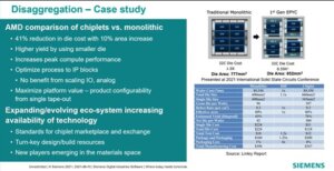
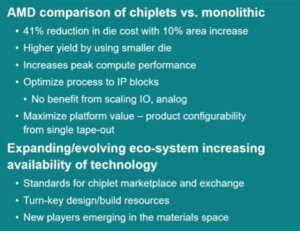
Felton uses the following AMD example of SoC vs chiplets:
The ultimate goal is for each company to build chiplets and sell them commercially as plug-and-play IP blocks to fabricate future circuits.
Chiplet suppliers face the following challenges:
- Transition to a system based co-optimization from design-based optimization
- requires consistent system representation throughout the design process
- Aggregation, visibility, and interoperability of cross-domain content
- Expanding supply chain and tool eco-system
- sharing and updating design content in a multi-vendor/tool environment
- do individual chiplet components work together as expected? – assembly-level verification
- Balancing design resources across competing multi-domain requirements
- recognizing the impact of early decisions on resource utilization, cost, and performance
- greater visibility into the impact of downstream effects earlier in the design process
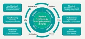
Siemens feels the use of chiplet technology/infrastructure will require true system technology co-optimization as shown in the flow below:

A lot of this design and standardization is being driven in Europe at Leti, Fraunhofer, and IMEC, more so than the US at the present time.
SiP Challenges for 5G Panel Session – Moderator Jan Vardaman – TechSearch
Karim of Amkor pointed out that 5G uses a lot of passive and active components, and to avoid increasing package size he is seeing a lot of double-sided assembly, in addition to the use of cavity-containing substrates to limit overall package thickness. Karim warned that excellent lab antenna designs did not always deliver when used in an actual phone.
Gerber of ASE added that the new frequencies that have been added expand the requirements from the RF front end. The phone suppliers also want more battery room so they are looking for more integration. At these higher frequencies antenna design becomes much more sensitive. Gerber also indicated that having different radios in the same module has created difficult shielding problems.
Vye from Cadence agreed that mm-wave designs now require integration of the antennas both in the package or on the chip. Special attention must be paid to electromagnetic analysis.
Liu from JCET pointed out the need for better control of both conformal shielding and compartmental shielding.
Braun from Fraunhofer IZM sees a strong emphasis on co-design where packaging must be considered early in the 5G design cycle.
For all the latest in Advanced Packaging stay linked to IFTLE…………………………..


