
I was halfway through my post about my day at Virtual SEMICON Taiwan, when I realized that to do the Global SiP Summit justice, meant it would need its very own post. The live version of the event spanned three full days. That’s a lot of content. While the on-demand version is abbreviated, you still get a great look at what is happening in this vibrant sector of the industry. These presentations are available until October 23. Let’s dive in.
AI on Chip Taiwan Alliance
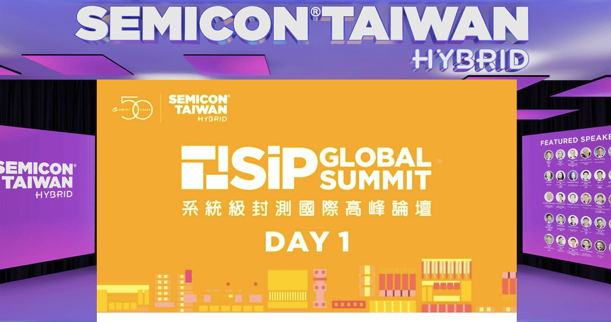
My goal at SEMICON Taiwan was to listen to the presentations I wouldn’t normally have access to, so I skipped over Jan Vardaman and Eric Beyne, imec — similar presentations have been covered recently on 3D InCites here, and here — and went straight to Shih-Chieh Chang, of ITRI, to learn about the AI on Chip Taiwan Alliance (AITA) a government-sponsored program (Figure 1).
AITA currently has 107 members, 11 of which are focused on packaging, and 20 of which are focused on system integration and applications. AITA’s goal is to create AI business opportunities, develop key technologies, and accelerate product development.
Chang said AI on-chip requires a solid supply chain, including memory and IC design and manufacturing, and packaging; security built-in; and IoT devices that address AI. According to Chang, Taiwan has it covered. He outlined a detailed technology focus that includes AI software, emerging architecture, heterogeneous integration (HI), and a domain-specific AI chip.
HI is key to the AI on Chip program, noted Chang, because it reduces form factor size 40-60%, reduces power consumption 25-40%, and improves performance 20-35%. Here again, bumpless chip to wafer hybrid bonding was identified as an enabling technology for AI chip HI.
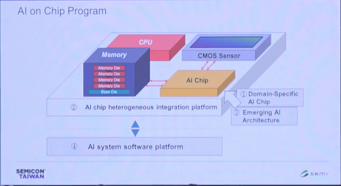
Chang also described a flip-chip embedded interposer carrier (FC-EIC), in which an interposer is embedded into the substrate or package to bridge two chips. It provides a flexible architecture for interconnection, is compatible with fan-out processes, and achieves close to 3DIC performance at a lower cost (Figure 2).
Substrates for HI
John Lau wrapped up Day one of the SiP Summit with a talk on substrates for heterogeneous integration, in which he defines HI, and then classified different HI substrates including organic, silicon interposers with and without through-silicon vias (TSVs), fan-out RDL, and ceramic substrates.
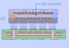
Lau provides some examples, such as Amkor’s automotive SiP that use organic substrates, and PCB-like substrates in smartphones. He also described how chiplet architectures have been used for both homogeneous and heterogeneous integration by showing different generations of AMD’s EPYC processor (Figure 3).
Much of his talk was dedicated to detailing the many different heterogeneous integration architectures that are either available or in development-many of them chiplet based.
Panel Level Package Ready for Take-off
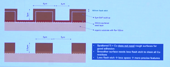
Stanley Low, of Evatec AG talked about Evatec’s panel level processes that are now available on the market. The company offers both wafer and panel-based solutions across the AP landscape, including wafer-level chip-scale packages, heterogeneous integration, and advanced IC substrate. For this presentation, Low focused on the company’s deposition capabilities, specifically addressing the challenges and requirements for seed layer deposition. He talked about the benefits of sputtering the Cu seeds vs. electroless copper seed, and detailed the degassing, etch and sputtering steps used and offered details about Evatec’s approach (Figure 4).
Solving Interconnect Processing Challenges
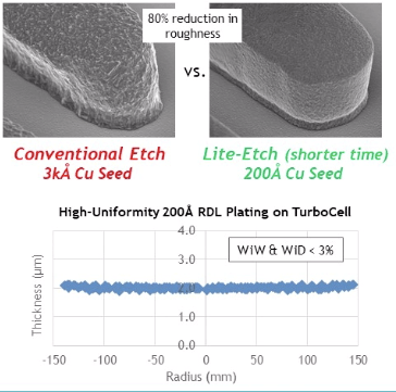
Lam Research’s Thomas Ponnuswamy, talked about challenges associated with the processing of interconnects in today’s HI applications. He explained how wet processes provide innovative and cost-effective solutions and talked about Lam’s suite of products designed to address that.
Ponnuswamy talked about processing copper pillars and stressed the importance of co-planarity. This is because meeting increased performance requires reducing bump pitch, which in turn tightens co-planarity specifications. Also impacting processes is die-level complexity due to increasing die size with more functionality. After describing the challenges in detail, he went on to discuss Lam’s solutions for coplanarity improvement. Moving on to high-density fan-out, Ponnuswamy discussed how signal integrity and of fine-line redistribution layers can be managed with Lam’s Lite-Etch and thin seed plating (Figure 5).
One key application that is gaining traction is Cu-Cu direct bonding, he noted. As it pertains to packaging, Ponnuswamy said the need arises when the pitch of pillars shrinks below 10µm. Key challenges of this application that can be addressed with wet processes include the need for low temperatures, pristine, smooth surface, and no height variation. Lastly, he talked about TSVs and the variation of via sizes. He said Lam’s process provides 100% void-free fill across a range of feature dimensions.
Next-Generation Advanced IC Packaging
Lincoln Lee, technical director for PacRim, of Mentor, a Siemens business, provided a design perspective of advanced IC packaging, particularly chiplets, and what Mentor is doing to address those challenges.
Lee explained that as device complexity increases over time, so too does the cost and risk of adopting new package technologies. (Figure 6).
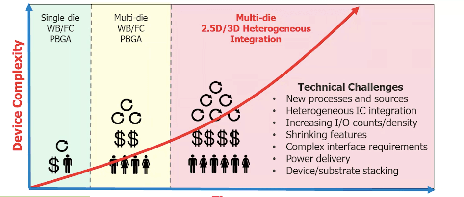
Verification challenges grow faster than the design size because there are more connections to check – the formula is N x (N-1). Despite challenges, he says high-density advanced packaging (HDAP) is still the fastest route to performance needed. He pointed out that the traditional packaging market is only growing in single-digit numbers, 2.5 and 3D heterogeneous integration is growing at 33% CAGR. This includes chiplets.
From the design perspective, explained Lee, the many challenges posed by chiplet architectures. He explained that this HDAP evolution is bringing disruptive change to our EDA tools, and outlined Mentor’s approach to supporting this with through its HDAP design kits and the establishment of the OSAT Alliance.
Cadence’s Julian Sun, also addressed the chiplet challenges from the design perspective. One key challenge he noted was the varied approaches to chiplet architectures as each tends to be vendor-specific. We still need a viable business model before IP companies can proceed with the mainstream commercialization of chiplets. He also noted ongoing work to define standards for chiplet-to-chiplet communication interface and data-exchange formats.
Like Lee, Sun stressed the importance of tools and workflows that support cross-domain design-team collaboration. He also described in detail, Cadence’s offerings that support ecosystem partnerships.
This wraps up my coverage of the SiP Summit. Don’t miss the upcoming IMAPS Symposium and the IWLPC, coming up this month, where we’ll learn even more about these vital topics. ~ FvT

