The Silicon Desert
Mar 30, 2026 · By Isabel Volpe · 3D In-Depth, R&D and Collaboration


Alchimer S.A. announced that its AquiVia deposition process is ready for implementation. AquiVia process can reportedly reduce overall cost...
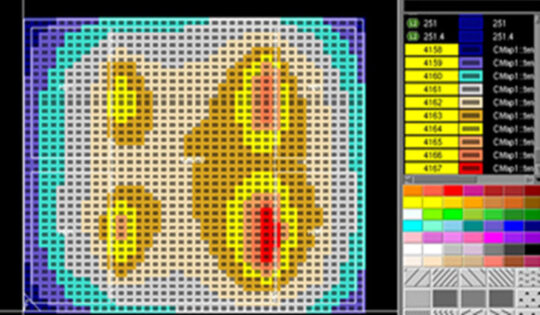
Metrology is consistently one of the more challenging areas in the semiconductor field. Whether it’s the monitoring of ultra-small...
Last year, it was all about through silicon vias (TSVs), this year, it’s all about everything else needed to...

Given the building momentum around 3D integration schemes and the attention it's getting as the semiconductor bright spot, it's...
The Jisso International Council (JIC) successfully completed its 10th annual meeting at the facilities of Minatec in Grenoble, France,...