
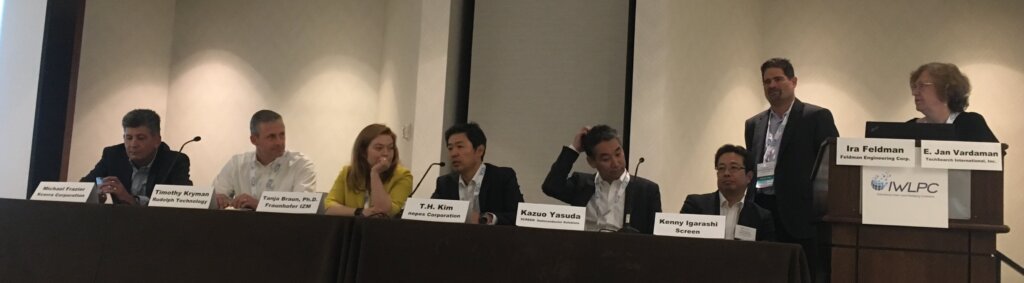
To the best of my recollection (and a quick search through 3D InCites’ archives) the panel level packaging (PLP) hoopla first hit the conference circuit in 2015 at the International Wafer Level Packaging Conference (IWLPC), when Jan Vardaman made it the topic of a panel discussion, and told a cautionary tale of following PLP down the rabbit hole. It seems that ever since, PLP has been an event headliner with keynote presentations and panel discussions at IWLPC 2016, IMAPS DPC 2017, ECTC 2017, and more. The dialogue continued last week at IWLPC 2017, which took place in the DoubleTree in San Jose, where PLP was the topic of both a keynote (Samsung’s Richard Bae) and a panel featuring Timothy Kryman, Rudolph Technology; T.H. Kim, nepes Corporation; Kazuo Yasuda, SCREEN; Tanja Braun, Ph.D., Fraunhofer IZM; Michael Frazier, Xcerra Corporation and co-moderated by Vardaman and Ira Feldman. It seems that PLP may just be the next sleeping giant for advanced packaging technologies. Or not. It depends on who’s talking and what’s at stake.
Team Panel vs. Team Team Wafer
As with every new technology (flip chip, through silicon vias (TSVs), and fan-out wafer level packaging (FOWLP) that threatens to disrupt the status quo, PLP is divided into two camps. I call them Team Panel and Team Wafer. Team Panel comprises mainly the OSATS, IDMS, substrate manufacturers, fabless companies who see the cost advantages of PLP; and a handful of equipment suppliers who have roots in flat panel display and solar technologies and are confident they can leverage existing equipment sets. Team Wafer comprises mainly the wafer tool manufacturers who recall the challenges and expense of developing tools for back-end wafer level processes, as well as the headache of transitioning from 200mm to 300mm wafers. Additionally, the materials suppliers lean towards Team Wafer, because they must figure out deposition techniques to accommodate panels vs. wafers. New to this panel discussion was the test community, who see the lack of standardization and the inability to probe 600×600 panels as reasons to be Team Wafer. For the past few years, the opinions of Team Wafer have prevailed, but this IWLPC panel discussion and keynote showed that Team Panel may be finally getting an edge, as they steadily poke holes in Team Wafer’s arguments.
It’s not that Team Panel doesn’t admit to challenges; they know there’s work to be done. It’s that Team Wafer has been burned before, particularly by the now mothballed transition to 450mm, and they will remain skeptical until they are sure developing tools will be worth the investment.
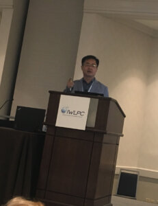
As nepes’ Kim noted, the question is whether a large panel format is competitive enough to capture the market. “Fan-out (FO) is already in volume production for round types. It’s more about competition than application type,” he said, “A new technology is always doubtful until you see it in volume production. (For most) PLP isn’t mature enough yet. Some customers are accepting this new technology and have engaged with us to start sample manufacturing.”
All agreed that the most urgent challenge is lack of standardization of panel sizes. Braun issued a call for participation in a survey put forth by SEMIs 3D Packaging and Integration Committee to help guide them in developing PLP standards.
What Team Wafer needs to remember, is that the 450mm wafer transition failure was primarily about economics, with essentially only four industry giants capable of backing tool development. Braun pointed out that moving to panel processing is not just about scaling technology from one wafer size to another. There are opportunities to develop new processes and materials across the entire ecosystem. She also said it’s not all about line and space requirements. Things like via sizes overlay and die shift issues need to be addressed, which also requires new or adapted tools.

Team Wafer may have been slightly more encouraged after listening to Bae’s keynote, who walked a tightrope to reveal just enough about Samsung’s successes with its “easy PLP” and plans to mass a chips-first version in Q1.18 for its own use. Bae dispelled some of the misunderstandings about the differences between FOWLP and FOPLP, noting that the materials, equipment, manufacturing environment, and final product are the same, and only the carrier shape is different. Samsung is developing both chips first and chips last approaches at 10µm line/space, said Bae, noting that below 10µm l/s, it’s no longer a packaging technology, it’s a semiconductor technology. He also said the end customer doesn’t really care about chips first or last; they only care about functionality, cost and device thickness. Beyond that, Bae kept a tight lid on any details that might reveal any Samsung trade secrets. He said all technical data will be revealed at ECTC 2018. (Save the date! May 29-June 1, 2018)
FOWLP – A Final Word
As one of the first OSATS to license and manufacture eWLB, one of the industry’s first fan-out technology, STATS ChipPAC’s BJ Han talked about the technology’s status, calling it the “true winner” of FO. He said we’ve entered the third wave for fan-out packaging, and that it became a mainstream technology without people even realizing it. Like Bae, he also dispelled a few misconceptions about the need for high-density fan-out. “People think we need fine line and space <1µm, and that’s not true,” noted Han. “5µm l/s is fine for the vast majority of applications, There’s only one application that calls for 2µm l/s.” He added that trying to provide better capability through costly high-end equipment is overkill because yield is everything in this game. Customers will find what is necessary for the market and find the line and space that is good enough. Han also said a solution provider must offer both wafer and panel-based capabilities.
Iyer’s Law
The only keynote NOT focused on FOWLP in some shape or form was delivered by Subramanian Iyer, of UCLA’s CHIPS program. A teacher at heart, Iyer always delivers a compelling talk. As I missed his keynote earlier this month at IMAPS’ 50th Anniversary Symposium, I was glad to have the opportunity to hear about the progress he’s having at the Center for Heterogeneous Integration and Performance Scaling (CHIPS), which is now caught the interest of DARPA, along with funding. While Herb Reiter covered the highlights here in his IMAPS blog post, I wanted to briefly address some details that weren’t included in that initial talk.
These days, everyone is talking about heterogeneous integration, and how it is the new scaling, but Iyer was one of the first to call it years ago. In this talk, he talked about re-engineering the package and the PCB, replacing the PCB with a silicon-based interconnect fabric, that Iyer says as much as it sounds like a silicon interposer, is much more. The idea is to design a whole system on a 300mm wafer, then singulate it into dielets, and re-integrating them onto the “interconnect fabric” at 2-10µm pitches. He calls it Moore’s Law for Packaging, but I think it should be called Iyer’s Law. This 300mm wafer populated with dielets replaces the entire PCB. Iyer explained this is not intended for hand-held applications, but to perhaps replace motherboards in servers, for example. A separate application Iyer described that could put the dielet concept to work using FOWLP to achieve biocompatible physically-flexible heterogeneous electronic systems used in neurological implants. This approach allows for the creation of a bicycle chain effect for true flexibility, in comparison with bendability of today’s flexible electronics solutions, which was very compelling. You can learn more about CHIPS at its next workshop, November 1, 2017.


Subu Iyer has been going around talking about Cu – Cu Thermo-compression Flip Chip Bonding as a way to shrink I/O pitch. What is the Cycle Time for his Cu – Cu TC or is that not of any concern to his funders at DARPA ? Or is his “Cu – Cu TC” in reality a Hybrid Bonding type process ( at Bonder quick Oxide || Oxide ==> off line slow anneal for Cu || Cu ) ?