


“It is better to be first than it is to be better.” (Ries and Trout, in The 22 Immutable Laws of Marketing.)
Or is it “Fast Followers Not First Movers Are The Real Winners?”
Fan-Out Wafer Level Packaging has built up such a head of steam this year (see “iPhone 7: Apple Charts a Strategic Course by Selecting TSMC’s inFO Platform”) that backwards reels the mind thinking about what comes next in advanced packaging, as next something surely will come, the new new thing.
After an ear-to-the-ground sampling last week at the lively International Wafer Level Packaging Conference 2016 in San Jose, CA, I have been thinking much about Fan-Out Panel Level Packaging and, particularly, thinking about the IWLPC Day 1 panel discussion I sat in on, a discussion moderated with gusto by Jan Vardaman, TechSearch International.
“The Role for Large-Area Panel Processing in the Quest for Low-Cost FOWLP” featured Bernie Adams, STATS ChipPAC Inc.; David Butler, SPTS Technologies; Choon Lee, Lam Research; Urmi Ray, Qualcomm Technologies, Inc.; and Chris Scanlan, Deca Technologies, who offered their perspectives and wisdom on the merits, or not, of Fan-Out Panel.
That, by my scorecard, was three customers (Deca, Qualcomm, STATS), two equipment suppliers (LRCX, SPTS), and one very savvy analyst (Jan).
Was a bit of sparring involved, were strong opinions shared, were definitive conclusions reached, was thinking swayed? Yes, yes, maybe, and … not really.
Was a technology ever shown less love than was Fan-Out Panel by the two equipment suppliers at IWLPC 2016? EUV Lithography comes to mind, although the lack of industry love there is coming more from the customer / device-maker side, put off by roughly a decade of delay in EUV’s commercial rollout, its HVM debut still not sure even at the 7nm process node, a checkered record indeed for a lithography method for which there was a strong need and pull as long ago as the 22nm days.
Fan-Out Wafer Level Packaging, by comparison, became a member of the HVM club so quickly, and by such unanimous consent, that it begs a much more detailed treatment than this one of FOWLP’s adoption ease contrasted with EUV’s insertion woes.
As for Fan-Out Panel Level Packaging, is it a case of “If you can’t be first in a category, set up a new category you can be first in?” (Ries and Trout, again).
Or is Fan-Out Panel truly bringing something extra to the advanced packaging party that will cause it to be greeted as a hail-fellow-well-met guest?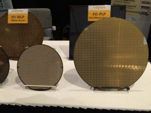
About Fan-Out Panel, I heard “I get the cost reduction,” from SPTS, about the economics of running large panels compared to relatively smaller wafers, “but you can’t get the yield to match [established Fan-Out Wafer Level processes].”
And, from Lam, “Yield at RDL is related to particle control.”
Making multi-RDL “a high-risk choice to go to panel.”
But about the economics, I also heard that for 10mm x 10mm and larger packages, Panel Level Packaging has the advantage, with something like a calculated 25% to 30% cost reduction when compared to Wafer Level. Another cost calculation shows that at 4mm x 4mm the cost lines cross for Panel Level and Wafer Level, with panels at an advantage for anything larger.
And I heard that the cost reduction for panel is higher as the complexity of the package increases. Think heterogeneous integration, for example.

When you do the math the world will run rather fewer panels than it would wafers if the Fan-Out world were to go completely to Panel Level Packaging, and, at present, there is no single standard for panel size but, per Qualcomm, many of the process tools needed for Panel Level Packaging are already available.
And Deca thinks the challenges going to HVM Panel Level Packaging are in need only of finding good engineering solutions; they don’t require inventing new science. (The state EUV Lithography still finds itself in, as I have heard repeated elsewhere, is that it continues to pioneer new science.)
Panel Level Packaging: we know how to do this, and by addressing engineering-only challenges the benefits are huge.
So, as a brave member of the audience asked the panel as the session concluded, will there be commercially available Fan-Out Panel Level Packing products on the market in October 2018?
“Yes; we are already making them.” (STATS ChipPAC.)
“Yes.” (SPTS.)
‘Yes, they will be available in the next 2 – 3 years.” (Qualcomm.)
“Yes.” (Lam Research, after a drawn-out answer that mostly skewed negative before concluding.)
“Probably.” (Deca Technologies.)
 Fan-Out Panel Level Packaging: whether or not it’s a First-Mover Advantage strategy, or one of Fast Follower, and despite the Debbie Downer take from the equipment suppliers this particular day, on this particular panel (Rudolph is much more upbeat!), cost is king, yields will follow, and the benefits are huge.
From Santa Clara, CA, thanks for reading. ~PFW


