
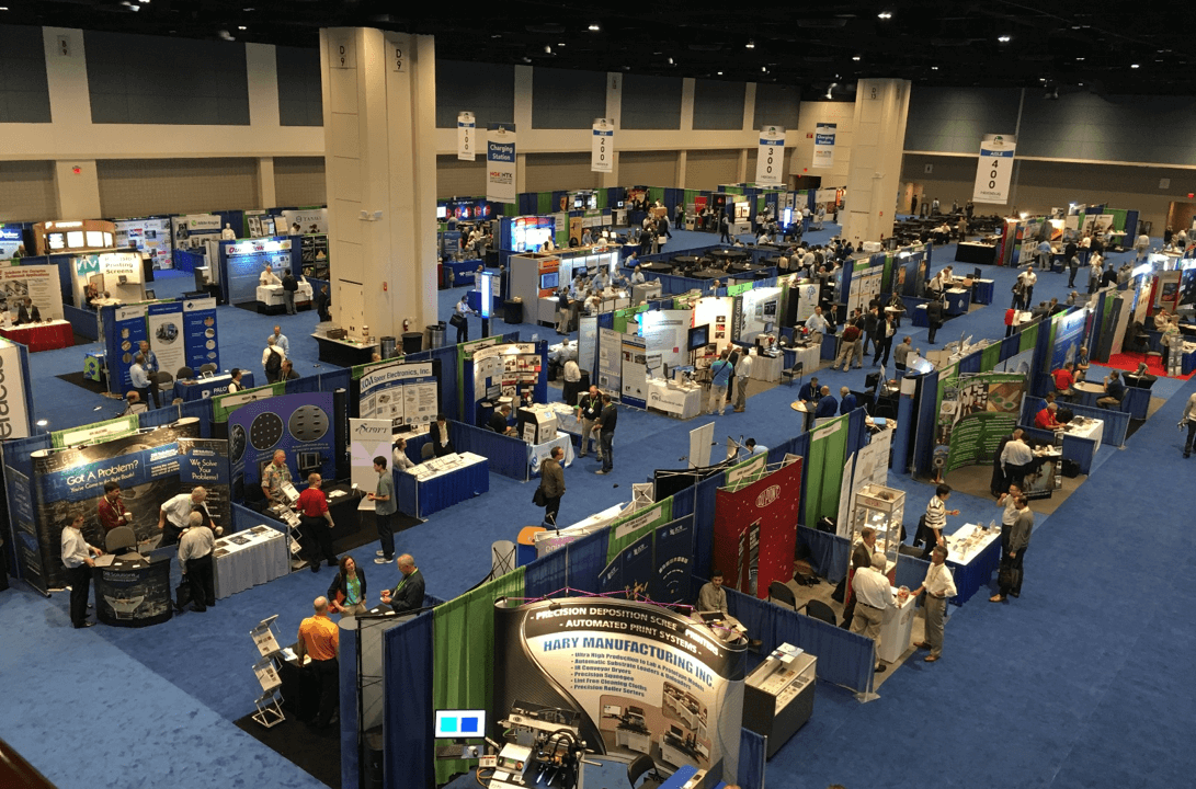

Almost 500 years ago Walter Raleigh was born in England, rose rapidly in the favor of Queen Elizabeth I and was knighted in 1585. In 1587 he initiated the founding of Raleigh. Last week he welcomed – appropriately dressed – about one thousand semiconductor experts to the 50th International Symposium on Microelectronics at the Raleigh, NC, Convention Center (Figure 1).
If you look closer at this photo, you’ll find that his “outfit” isn’t suitable for class 1 wafer fabs, but kind of acceptable for less demanding cleanrooms, like the ones widely used at IC assembly & test facilities. That’s intentional because the IMAPS event was focused on the rapidly expanding IC packaging segment within the semiconductor industry.
Before we look at individual sessions, a few words about a common theme: I clearly noticed in many presentations: Die – package – board electrical, thermal, mechanical and chemical interactions and their impact on reliability. That’s a swift response to the demands of automotive applications, today’s fastest growing semiconductor market. I am happy to see that the IC manufacturers are responding so quickly to the automotive industry’s pressure for ZERO defects. I just hope that the EDA and IC design experts will soon offer their contributions to guarantee system safety and security while keeping cost low. EDA tools and design methodologies for system-level planning, logic redundancy, self-repair, system-level test, multi-physics simulation and other productivity tools can/could significantly reduce NREs and time to market. Also, IMAPS 2017 showed me that the stringent automotive requirements are likely to intensify the cooperation between design and manufacturing experts.
As usual, on day one, Monday, Oct 9, IMAPS offered professional development courses (PDCs), this year in four tracks. Each one of these 2-hour PDCs focused on an important materials, equipment or manufacturing topic. In addition, conference attendees could join a tour to the advanced interconnect technology (AIT) Division of Micross. Arriving from California at midnight on Monday, I, of course, missed the entire day one program.
On Tuesday morning, this year’s IMAPS’ President, Susan Trulli, and General Chair, Dan Krueger, welcomed the large audience, thanked the many organizers and contributors of this event, outlined the 2017 program and announced the dates for Pasadena’s 2018 and Boston’s 2019 conferences, to be held Oct 8 to 11, and Sept 30 to Oct 3, respectively.
Ahmer Syed, Senior Director, Package Engineering, Qualcomm Technologies, Inc. was our first keynote speaker. Syed conveyed several key trends he observes in his role at the largest supplier of smartphone components: 1) The phones are getting thinner with every model year 2) Battery capacity is increasing steadily 3) The room for PCB and electronic components is getting tighter — demanding ever higher levels of integration 4) Thickness of printed circuit boards is decreasing.
As shrinking transistors is becoming more and more expensive and very risky, IC packaging technologies are taking over as primary drivers of form factor shrinking. IC packages get thinner (Z), as MEP replaces molded leadless package (MLP) technology, and smaller in X and Y directions as copper studs replace solder bumps. These tighter pitches on IC packages drive advancements in PCB technologies and demand die – package – board CO-design methodologies and tools. With increasing signaling frequencies, more IC packages now require shielding. Last, but certainly not least, Syed asked the audience for many more levels of integration so they can pack today’s 400 to 500 active and passive smartphone components into ONE IC package.
It’s my belief that progressing towards this aggressive goal will shift a major part of the value creation from the system to the component level and will simplify the supply chain – from a system vendor’s perspective – significantly. It will also shift value creation from the individual die(s) to the IC package and give assembly & test houses plenty of opportunities to grow. If you have seen, like me, the transition from individual transistors, resistors, diodes, etc. to today’s SoCs, you’ll find Syed’s request very logical and quite reasonable. Let’s accept this challenge and review our progress in 2030!!!
The next keynoter showed us how to immediately achieve these higher levels of integration using today’s technologies. Subramanian S. Iyer, former IBM fellow, now Distinguished Chancellor’s Professor at UCLA, and Director of the Center for Heterogeneous Integration and Performance Scaling (CHIPS) titled his presentation: Packaging without the Package – A More Holistic Moore’s Law.
Iyer pointed out that our industry doesn’t only need much higher levels of (homogeneous) integration, but also an economical and relatively quick way to pack heterogeneous functions (logic, memory, analog, RF, MEMS, sensors, …) into ONE IC package. He reminded us that Gene Amdahl founded Trilogy in 1980 to pursue wafer-scale integration. While the design and process technologies available at that time didn’t allow Amdahl’s concept to succeed, Iyer showed that his CHIPS strategy relies on many currently available technologies, is much more flexible and useful than Amdahl’s approach and, to my surprise, has made a lot of progress since I last heard Iyer’s presentation earlier this year. By combining bare dies, called “dielets” (a.k.a. “chiplets”) on a silicon interposer and utilizing today’s tight interconnect technologies (<1µ L/S), very high levels of integration for heterogeneous functions can be achieved with proven assembly technologies. We, of course, need to expand the library of dielets and passive components, refine die placement, interconnect and test methodologies and develop additional tools and flows for die-level IP re-use, planning, and design of such “Superchips”. Then, tiny and extremely low power smartphones, wearables, IoT edge nodes, etc. will demonstrate the power of system scaling and transform our industry from the current low margin component focus to a much higher margin (sub)system solutions provider.
After a short coffee break to let the importance of Iyer’s impressive message sink in, Benjamin Leever, Senior Materials Engineer, Air Force Research Laboratory, Soft Matter Materials Branch, took the stage. He talked mostly about an organization driving technology development for system scaling: Nextflex. In 2015 it began to invent and mature manufacturing technologies for flexible hybrid electronics (FHE). With currently 80 members and 13 public-private partnerships they are developing manufacturing technologies for printing circuits and placing dies onto flexible substrates to assemble electronic systems. What to do with FHE technology? The small form factor, low-power dissipation, and low cost make them perfect for tracking and/or monitoring of all kinds of assets, e.g.: A pilot’s vital signs, as well as a plane’s many components. This will enable preventive maintenance of both “man and machine”. Nextflex also contributes significantly to educating our next-generation manufacturing workforce, facilitates member-driven road-mapping and coordinates industry-wide efforts, such as suggesting design methodologies and best practices for manufacturing flows – but has no plans to impose standards.
Compared to the previous keynoters, Tim Olsen, founder and CTO of Deca Technologies, got very specific. He described how Deca’s M-series assembly technology contributes to enabling accurate placement of dies and fine-pitch interconnects – to narrow the gap between nanometer geometries on dies and 10s and 100s of micrometers in today’s IC assembly. Deca’s adaptive patterning technology will enable 2m L/S interconnects and highly accurate die-placement to save area and cost. ASE’s $ 60M investment in Deca shows how interested the #1 assembly house is in this technology. ASE’s engagement will certainly accelerate market acceptance of this technology.
Urmi Ray, IMAPS’ VP of Technology and Mary Christina Ruales Ortega, the 2017 Technical Chair, outlined some conference logistics topics, invited the attendees for lunch and opened the exhibition.
Starting Tuesday afternoon, the conference offered five parallel sessions. For my EDA-centric work, I found the session chip – package interaction (“CPI”) most useful and spent a major part of my time in this session. Other sessions focused on high-performance manufacturing challenges, advanced and enabling technologies, and system integration and materials.

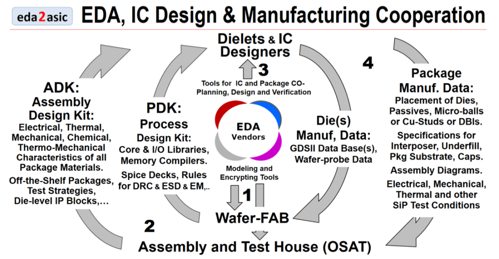
At this conference, I also had the opportunity to convey my focus in a 20-minute presentation: Highlighting the importance of a user-friendly multi-die IC design ecosystem and encouraging EDA, IC design, manufacturing and test experts to communicate and cooperate more closely. Based on my many years of program management experience at ASIC and EDA companies, I have seen how important accurate and up-to-date process design kits (PDKs) are for the successful cooperation between IC designers and their wafer-foundry partner. I also observed how many IC designs were “thrown over the wall” to the IC packaging partner, to make it work – somehow. However, they bounced — like a ping-pong ball — multiple times back and forth between IC designers and packaging experts. Considering how many engineering resources and how much time this ping-pong game may consume, I suggest developing Assembly Design Kits (ADKs) to parallel the proven PDKs and enable equally efficient cooperation between IC design companies and assembly & test houses. Figure 2 shows my 4-step diagram:
This “ADK Business Model” will also enable the OSATs to develop “off-the-shelf”, easily customizable packaging platforms. They’ll save both customer and supplier significant development cost and minimize their time to profit. When cell-phones demanded millions of units per month, fully custom IC packaging made sense. However, as many future applications will never reach such volumes, reducing development cost and getting to market faster will become much more important for the success of all parties involved.
I also had the opportunity to participate in the poster session on Thursday noon. I am glad I invested in combining my slides in a pretty poster because several very experienced IC packaging managers expressed interest in my push for a complete ecosystem and especially my ADK missionary work. They offered me their support and gave me new ideas for making my work more effective.
Instead of detailing dozens of very good presentations on several more pages, and exceeding the limits of a blog, allow me to focus on two presenters that impressed me a lot. They clearly conveyed the value proposition of advanced packaging for single and multi-die ICs. They also explained major manufacturing challenges and the importance of EDA tools to simulate the effects of CPI or CBI (Chip-package and Chip-Board-Interactions).
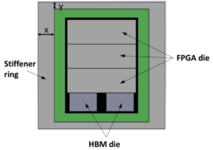
Xilinx was the first semiconductor vendor to demonstrate the cost, power, performance and form-factor benefits of combining four FPGA slices in one IC package. In the past 10 years, Xilinx created a whole family of multi-die ICs targeting specific applications. Xilinx’ Jaspreet Gandhi explained the value proposition of one of their latest parts, combining 3FPGA slices with two high-bandwidth Memories (HBMs) (Figure 3). He explained that data centers like to use this FPGA and HBM combo to off-load compute-intensive tasks from a processor to FPGAs to save time and power. The proximity of logic and memory in this multi-die IC offers 10X the bandwidth and 4X lower power compared to a bank of DDR4 memories surrounding a FPGA. Gandhi pointed out that ideally, HBMs should match logic temperatures and allow 105°C junction temperature. Because DRAMs don’t, HBMs have, like FPGAs, temperature sensors built in and throttle performance when needed to avoid functional or performance failures or reliability problems.
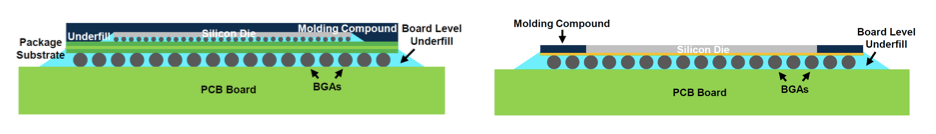
Smartphones need to get thinner – as Qualcomm’s Ahmer Syed stated in his keynote. It’s no surprise that components also need to get thinner (less in Z-direction). Qualcomm’s Mark Nakamoto described the technical challenges, as height restrictions suggest elimination of the package substrate and demand direct mounting of a die onto a PCB (Figure 4). The picture on the left shows a die – package – board configuration and the importance of underfill to mitigate stress due to different coefficient of thermal expansions (CTEs). When directly mounting dies onto the PCB, the board-level underfill becomes even more important. In addition, PCB limitations demand much wider contact spacing between the die and the PCB.
Two more important points about IMAPS 2017:
- More than 100 exhibitors showed their materials, equipment and manufacturing capabilities, and discussed opportunities for cooperation with potential customers and partners. I was very happy to see that Cadence had a booth too!
- On Wednesday evening, we had a number of IC packaging experts facing questions from Jan Vardaman (TechSearch Inc) and Gabriel Pares, (CEA-LETI) as moderators and from several hundred people in the audience.
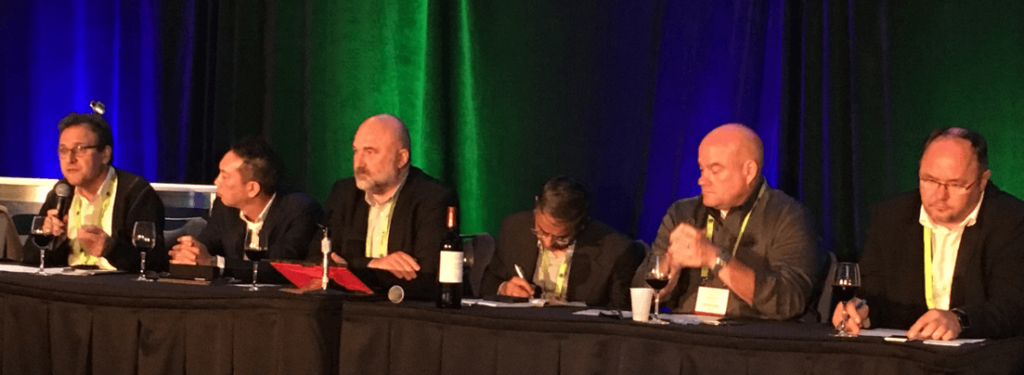
The Panel’s title was: “Global Perspectives on Packaging requirements and Trends towards 2025”. It triggered right away questions about the G5 communications standard and a discussion if even higher frequencies (77 to 81 GHz) for Lidar applications in automotive will demand totally different materials. It became quickly obvious that both applications will be very cost-sensitive and put cost pressure on new, still to be developed, materials. Like many presenters during the entire conference, the panelists also emphasized the increasing importance of component and system reliability. GeorgiaTech’s Sundaram even said: “We’ll need aerospace reliability at smartphone cost”.
The muted reaction to my EDA centric questions demonstrated that I’ll still have plenty of work to do to bridge the gap between EDA & IC designers and their IC manufacturing & test partners.
~ Herb


