June 2025 was a notable month for the semiconductor industry, featuring significant progress in materials innovation, strategic partnerships, and market development. Key advances included breakthroughs in additive electronics and 2D materials, along with collaborations aimed at enhancing power electronics and industry insights. Events and initiatives highlighted the importance of supply chain resilience and regional manufacturing growth, while new platforms and packaging solutions addressed evolving technology demands. Overall, the month demonstrated our member companies’ ongoing commitment to innovation, collaboration, and building a stronger semiconductor ecosystem.
Technology and Innovation
Siemens introduced a new AI-enhanced toolset for the EDA design flow at the 2025 Design Automation Conference (DAC). The system, developed specifically for semiconductor and PCB design environments, is intended to improve productivity and shorten time-to-market through the use of generative and agentic AI. Siemens highlighted integration of NVIDIA’s NIM microservices and Llama Nemotron models to support these capabilities. The company is reportedly embedding AI across its portfolio, including Aprisa AI, Calibre Vision AI, and Solido tools. Early access to the new system is available.
Nordson Electronics Solutions collaborated with Powertech Technology, Inc. to develop a panel-level packaging solution that achieves underfill yields exceeding 99%. Utilizing the ASYMTEK Vantage® Dispensing system equipped with the IntelliJet® Jetting system, this innovation reduces underfill voids and decreases cycle time by nearly 30%.
Brewer Science showcased its advancements in additive manufacturing materials at TechBlick 2025 in Boston. The company highlighted its development of printable dielectric materials and functional inks designed to enable the integration of complex 3D traces and embedded functions directly into electronic devices. These innovations aim to reduce costs, enhance design flexibility, and support a more resilient domestic supply chain for advanced packaging.
SEMI reported a 21% year-over-year increase in global semiconductor equipment billings, totaling $32.05 billion in Q1 2025. This growth is attributed to sustained demand for artificial intelligence (AI) applications and ongoing fab expansions worldwide. Despite a typical seasonal dip of 5% quarter-over-quarter, the industry remains resilient, with investments in chipmaking capacity continuing to rise. SEMI emphasizes the importance of policy stability to support these multi-billion-dollar investments and the long-term success of advanced manufacturing operations.
StratEdge Corporation commemorated its 40th anniversary at the International Microwave Symposium (IMS) 2025, which showcased its high-reliability ceramic packages used in telecom, defense, 5G, and aerospace applications. The company highlighted its history of packaging solutions, including components utilized in Mars rovers, underscoring its commitment to advancing semiconductor packaging technologies.
Collaborations and Acquisitions
Siemens expanded its collaboration with Samsung Foundry, extending certification of its EDA tools across Samsung’s advanced FinFET and MBCFET nodes, including SF2 and SF2P. The agreement covers Siemens’ Calibre, Solido, and Aprisa software, aiming to support reliable design for next-generation semiconductor devices. In addition to certifications, both companies introduced joint solutions targeting design challenges in areas such as power integrity, silicon photonics, and analog mixed-signal verification. The collaboration is intended to enhance design capabilities for competitive markets and evolving 3D-IC architectures.
Indium Corporation joined the Center for Power Electronics Systems (CPES) Industry Consortium at Virginia Tech to contribute to cutting-edge research in power electronics. This partnership is intended to support advancements in power device packaging, thermal management, and materials science aimed at improving energy efficiency and system reliability. Indium’s involvement provides access to collaborative R&D resources and facilitates the translation of research into practical industry applications.
SEMI announced the acquisition of select assets from Linx Consulting, LLC, including its market reports and conferences. The move is intended to enhance SEMI’s Market Intelligence capabilities, particularly in specialty materials and manufacturing processes. According to the organization, the integration of Linx’s expertise in semiconductor and electronics materials market analysis is expected to support more robust insights for SEMI’s global membership.
Kiterocket was named agency of record for SEMI, marking a new collaboration aimed at supporting the organization’s communications on global policy, workforce development, and industry trends. The partnership is intended to enhance SEMI’s outreach during a period of heightened visibility for the semiconductor industry.
Expansion and Development
Evatec updated its website with a newly expanded Markets section. The update replaced five broader categories with more detailed segments such as Power Devices, MEMS, Wireless, Wafer & Panel Level Packaging, and Wafer Level Optics, among others. Each market page outlines relevant applications, technologies, and production solutions. Additional page updates are expected to follow.
SurplusGLOBAL initiated the beta phase of its new AI-driven platform, SemiMarket, designed to streamline the buying and selling of semiconductor equipment and parts. This platform aims to enhance the efficiency of global transactions by offering a user-friendly interface and advanced search capabilities. The grand opening is scheduled for December 2025, transitioning eSemiMarket into a fully operational, seller-driven marketplace.
Awards and Recognition
ACM Research’s Chief Technologist Sally Ann Henry was recognized on International Women in Engineering Day, highlighting her professional journey and impact on the semiconductor industry. Her career has been defined by mentorship, curiosity, and cross-cultural collaboration.
Evatec was recognized as an “excellent supplier” during Silex’s 10th anniversary celebration held on May 14. The award acknowledged the companies’ longstanding partnership and shared commitment to quality. Evatec’s Henfy Su delivered remarks at the event, reflecting on Silex’s ten years of innovation and their collaborative progress.
Fraunhofer IZM awarded Dr. Lutz Stobbe the 2025 Fraunhofer IZM Research Award for his work in sustainable microelectronics. He was recognized for his research on the life cycle assessment of ICT infrastructures, including data centers and network technologies. His findings aim to support more environmentally responsible digital infrastructure. Dr. Stobbe’s career path—beginning in Japanology and progressing into microelectronics through technical translation—reflects an interdisciplinary approach to sustainability in technology.
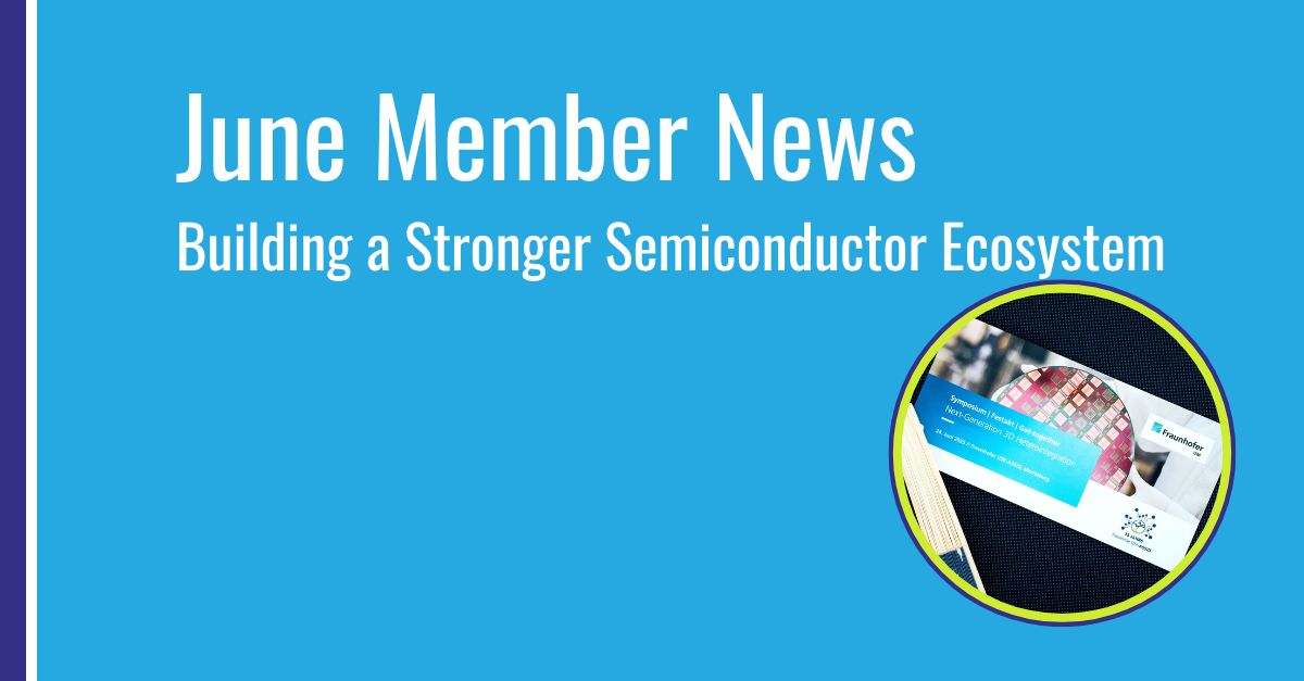
Fraunhofer IZM-ASSID celebrated its 15th anniversary on June 24, 2025. in Moritzburg, Germany with a symposium and a festive event. Since its founding in 2010, the Saxony site has become a globally recognized engine of innovation in 3D system integration and wafer-level packaging. From the development of novel Through-Silicon Vias (TSV) to innovative chip stacking solutions, they continue pushing the boundaries of microelectronics.
Industry Events
EV Group participated in the 2025 ITF World event in Antwerp, where Executive Technology Director Paul Lindner contributed to the NanoIC pilot line workshop. The session featured presentations and panel discussions focused on the technologies targeted by the pilot line and how stakeholders can engage with its capabilities. The workshop highlighted efforts to advance innovation across Europe’s semiconductor landscape.
EVG also participated in the 42nd International Conference of Photopolymer Science and Technology, presenting developments in lithography and nanoimprint technology. On June 26, Ksenija Varga delivered a presentation on digital lithography for SWIR applications, focusing on the use of EVG’s LITHOSCALE® Maskless Exposure Technology and novel IR-pass resists. The talk, co-authored with FUJIFILM Electronic Materials, highlighted advancements in stitch-free, full-wafer structuring and improved critical dimension (CD) uniformity.
ERS electronic GmbH[s Advanced Packaging Product Manager, Wenxuan Song, attended the Fan-out Panel Level Advanced Packaging Forum (FOPLP2025) on June 27 in Shenzhen (CEST). The company showcased its latest panel-level packaging solutions and discussed ongoing efforts to advance innovation in the field.
ERS also participated in SWTest San Diego, where CTO Klemens Reitinger co-presented with watttron’s Klaudiusz Holeczek on a joint solution for full-content wafer testing of high-power chips used in AI and high-performance computing applications. The session highlighted efforts to support evolving semiconductor test requirements.
SEMI’s SEMICON West 2025 will be hosted for the first time in Phoenix, underscoring Arizona’s growing importance as a semiconductor manufacturing hub. The event aims to showcase regional capabilities, including advanced packaging, chip fabrication, and materials innovation. Organizers expect the gathering to bring together industry stakeholders, government representatives, and researchers to foster collaboration and investment in the local semiconductor ecosystem.

IMAPS’ CHIPcon 2025 conference takese place July 7-10 at the Marriott in San Jose, California. The event will focus on chiplet technologies, including integration methods, advanced packaging, and emerging device architectures. Industry leaders, researchers, and suppliers are expected to gather to share insights on semiconductor performance trends and supply chain innovations. The conference provides opportunities for networking, collaboration, and exposure to the latest developments shaping the future of semiconductor packaging and assembly.
The SEMI 3D & Systems Summit, held June 25–27, 2025, in Dresden, Germany, focused on the theme “Heterogeneous Integration: Bolstering Europe’s Resilience.” The event brought together industry leaders to discuss advancements in chiplet applications, hybrid bonding techniques, and the integration of diverse materials and processes to enhance semiconductor performance and sustainability. Keynote speakers included representatives from 3D InCites member companies such as Adeia, ASE, Comet Yxlon, EVG, and KLA, who shared insights on topics ranging from AI semiconductor systems to co-packaged optics and workforce development.
Saras Micro Devices announced its team will participate in the 5th International Symposium on 3D Electronics Integration & Manufacturing at the National Renewable Energy Laboratory. The company aims to engage with technical experts and industry stakeholders to discuss recent developments in 3D power electronics integration and manufacturing.
NHanced Semiconductors’s Vice President Charles Woychik is scheduled to deliver a keynote address at the upcoming Surface Mount Technology Association (SMTA) symposium focusing on counterfeit parts and materials. The event, taking place in College Park, Maryland, will address challenges related to supply chain security, component authenticity, and mitigation strategies.
Workforce Development
Saras Micro Devices welcomed a cohort of summer interns, aiming to foster professional development through hands-on learning and collaboration. The program is intended to provide students with practical experience while contributing to the company’s ongoing initiatives. Interns are expected to bring new perspectives to the team over the coming months.
SEMI Europe announced GENESIS, a collaborative initiative uniting 58 research institutes, universities, and industry leaders to drive sustainable innovation in microelectronics manufacturing. As the lead of Work Package 6 (WP6), SEMI Europe focuses on regulations, dissemination, communication, and exploitation to ensure GENESIS outcomes effectively reach key stakeholders and support EU sustainability objectives. Coordinated by CEA-Leti and backed by Chips JU, member states, and Switzerland’s SERI, GENESIS aims to build a resilient, circular, and green semiconductor ecosystem in Europe, in line with the European Chips Act and the Green Deal.
Career Advancements and Opportunities
SEMI’s FlexTech community issued a Request for Proposals aimed at advancing flexible hybrid electronics (FHE) technologies, focusing on the development of advanced materials and additive processing.Key areas of interest include advanced materials, integrated digital twin platforms for multiscale and multimaterial additive electronics manufacturing, system integration, reliability, and standards for scalable FHE production. Additional restricted topics cover market and application landscape assessment, process development kits for FHE, and 3D geometry and co-design tools. White papers are due by July 14, 2025.
Veeco has multiple hirings available including,
Senior Quality Engineer in Horsham, PA. Linked here.
Mechanical Engineer of Fluidics in Horsham, PA. Linked here.
Field Service Engineer in Nakuru, Kenya. Linked here.
Amkor Technology has an Internship Opportunity in Teluk Panglima Garang, Selangor in Amkor Malaysia. Linked here.
Onto Innovation has two hirings available including,
Staff Electrical Engineer in Milpitas, CA. Linked here.
Configuration and Release Engineer in Bloomington, MN. Linked here.