
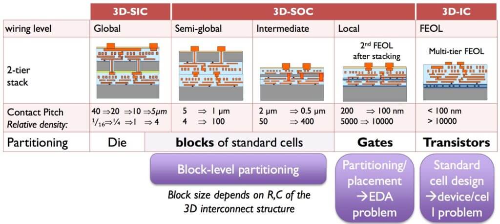
As scientists, we have a tendency to classify and categorize. It’s our way of comparing and contrasting things in our world. Some of these classifications stick and some don’t. For instance at the start of 3D a decade or so ago, Eric Beyne of IMEC laid out a perfectly reasonable classification of 3D structures based on the level of interconnect they were making. [ Link] It made all the sense in the world and still does, but no one really is using this nomenclature (Figure 1).
Recently at the International Microsystems Packaging Assembly and Circuits Technology (2018 IMPACT) conference in Taipei, Taiwan, DC Hu of SiPlus gave a presentation entitled “Electronic Packaging Solutions for Artificial Intelligence Applications” What caught my attention was DC’s attempt to categorize high-performance packaging by structure, or as he put it “Many terminologies are used to describe high-performance computing (HPC) packaging. This may confuse users. A new classification of HPC packaging by structure is proposed for the first time by the author. This is a bit complex so try to stay with my discussion. His premise is that there are only eight possible structures as shown in Figure 2.
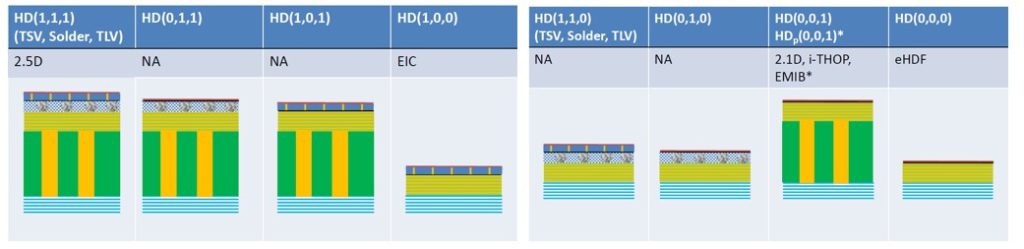
If we look at which structures are commercial or are being scaled up they are the following, as shown in Figure 3:
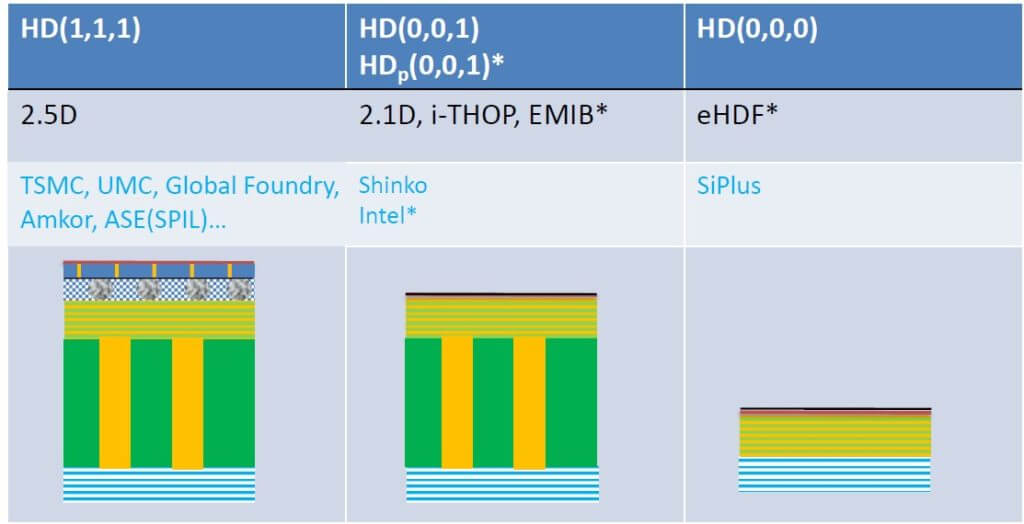
Their embedded high-density film (eHDF) process is probably the least well known of these structures. eHDF is a connection of two/three types of “substrate” technologies (Interposer, substrate) without solders in-between. Each “substrate” technology (Interposer, substrate) does not have TXVs. ( Through Silicon Via, Through Laminate Via, etc.).
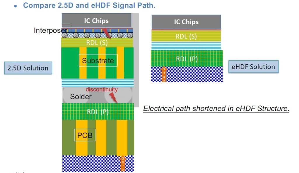
Comparison to standard 2.5D technology is shown in Figure 4. One can see a much thinner solution and because of the fewer interfaces, this should give the best electrical performance.
SiPlus claims a potentially lower cost structure because:
- There are no silicon (TSV) and laminated cores(TLV).
- Compared with 2.5D, only half of the total interposer and substrate surface finishing is needed.
- Solder between the Interposer and the substrate (Intra-solder) is eliminated.
- logistic and testing is simplified.
SiPlus reports that they are working with mass production partner to bring this technology to commercialization. Will this new way to categorize high-density packaging catch on and become accepted nomenclature?? Only time will tell.

Yes, that’s right ….A TRILLION UNITS
For those of you that have not seen the headline yet, IC Insights reports that we achieved a significant manufacturing milestone in 2018 – the production of 1 trillion integrated circuits (ICs).
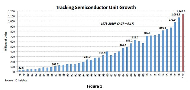
To put that into perspective we (the industry) were approaching 100B units when I really started paying attention in 1985. The technology argument of the day was whether surface mount technology would really make a dent in the through-hole assembly market. Would the industry really spend the monies to put lines in place for this new assembly technique? In the ensuing 35 or so years we have grown 10X or about a doubling of unit growth per decade.
For all the latest in advanced packaging stay linked to IFTLE………………………………


