


At last week’s third edition of the European 3D TSV Summit, over 250 attendees from 22 countries gathered at Minatec Campus in Grenoble, France to talk about how 3D enables smarter systems. The discussions seemed to picked right up from where we left off at the 3DASIP Conference in December and the GIT Workshop in November.
Cost is a matter of perspective
While Qualcomm is still waiting for interposer and 3D integration in its HVM products, AMD is ready to roll. Why the disparity? For both companies, cost is the motivator. But Qualcomm is comparing cost to package-on-package (PoP) solutions, its go-to for mobile memory on logic. For AMD, the comparison is with the cost of SoC scaling, and the improvement in cost per transistor that die stacking can get you.
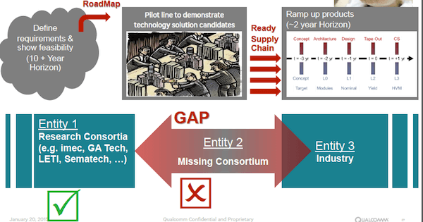
According to Mustafa Badaroglu, Sr. Program Manager, Qualcomm, the company is still waiting for a low cost solution for memory on logic. For now, package-on-package is the go-to technology. They haven’t reached the product intercept yet. While he called split die a “no-brainer” for large die products, such as FPGAs, “For mobile we use cheap packages.” he explained. “Cost is king. It trumps all other value propositions for existing products.” He noted that technology development cannot be driven by product commitment. “To leverage a disruptive technology, a product must be architected for it,” he said. As such, Qualcomm is leading efforts to establish an industry consortium to define and use what they call “concept architectures” analogous to concept cars (Figure 1). The goal is to provide “a graceful runway for deploying disruptive package-based more than Moore (MtM) technologies.”
Bryan Black, AMD Fellow, offered his opinion on why die stacking is happening at AMD now rather than 10 years ago. “We had figured out how to do it, and had figured out yield issues, but it wasn’t time. Now it’s time.”
With regard to the disparity on cost between AMD and Qualcomm, Black said It all comes down to the average selling price (ASP). “The big iron pays for new technology,” explained Black. “The big iron has a much larger ASP. 2OK ASP can do a lot of technology.” The challenge for Qualcomm, as Black sees it, is in building a million phones a day. Die stack solutions just aren’t possible for that infrastructure.
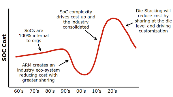
Black’s keynote focused on the advantages of SoC disintegration into functional blocks at optimal node, and using interposer or 3D IC configurations to integrate them. “For me, there’s no difference between interposer or vertical stacking,” he said. “They both have the same manufacturing and test challenges. If I put one transistor on an interposer it’s a 3D stack. I believe they have different uses in the market and will co-exist.” He provided the following graph to explain how cost has always driven the next generation of SoCs.
In his keynote, Timo Hentonnen concurred with Badaroglu, saying that it still remains to be seen if 3D TSVs will ever make it to mobile processors. “It is certainly doable but can we bear the yield and cost, and what benefits can it offer?” he asked. He said PoP will continue to scale to 0.33mmP, enabling higher pin counts. What needs to happen then is solving the yield and cost challenges. We also need to develop wafer test technology to enable known-good die (KGD) and true 3D ICs. And lastly, he said thermal management aspects need careful consideration.
Hope for Smarter Systems
For Martin Schrems, VP of R&D at ams, TSVs should not be viewed as “evil.” “There are two ways to do it. You can try and make TSVs cheaper. The other way is to look at what you can integrate,” he explained. “TSV cost doesn’t matter if you can integrate more. In our experience, it’s a good path to success.”

Schrems spoke from the point of view of a medium size IDM. For ams, there’s lots of promise using via last die-to-die stacking in niche applications. He talked about 3D sensor integration for smarter systems, and the doors 3D TSV opens for it. He explained that to become smart, the system needs to understand the environment. It all starts with sensors, in addition to wireless receivers, interfaces, and data processing. “Everything we do in semiconductors is needed for smart systems,” said Schrems. “Packaging becomes more expensive because we have more blocks to combine. 3D adds hope for reduced cost at the system level.”
ams’ first 3D product is an intelligent light sensor that enables energy savings for displays, lighting and in the phone. What drives 3D in this application, says Schrems, is low package height, and the elimination of glass enables thinner devices and improved optical performance. “40% of a system’s power comes from the display,” he noted. “Ambient light sensors can reduce overall power consumption by 30%.” For smart phones, this is a great advantage. Schrems also discussed the promise 3D holds for chemical sensor systems, and 3D integration for photonics, and healthcare applications.
One question for Schrems was whether there will still be room for niche applications when the big volumes are there. Schrems assured him they would support both small and large volumes. I imagine that would be a good problem to have.
Everybody agrees…
And so the discussions continue to go around and around…. everyone agrees that 3D is happening now, albeit only in high-end computing applications, thanks to memory stacks and interposer integration. Its generally agreed that to migrate to mainstream consumer products, the cost needs to come down for both interposer and 3D IC technologies, although there is disagreement as to whether we just let this happen as a matter of course, like its predecessors, or whether a consortium is needed to help it along. Then there are those who promote developing active interposers as a way to justify the added costs. The latest new discussion that started at the GIT Workshop in November, continued through 3D ASIP in December, and got picked up again at the 3D TSV Summit is the idea that a concept application might be what’s needed to ramp 3D ICs to high volume manufacturing (HVM) in consumer products. ~ F.v.T.


