Search Results

Matches for your search: "fan-out wafer level packaging "

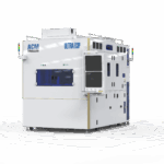
ACM Research Delivers First Horizontal Panel Electroplating Tool Strengthening Its Leadership in Fan-Out Panel-Level Packaging

ACM Research, a leading supplier of wafer and panel processing solutions for semiconductor and advanced packaging applications, today announced it has delivered the first panel electrochemical plating tool, the Ultra ECP ap-p, to an industry-leading panel fabrication customer. This achievement underscores ACM’s advancement in panel-level electroplating technology and reflects growing...

SEMICON West Member Preview 2025

After more than 50 years in San Francisco, SEMICON West is making its debut in Phoenix, Arizona! As Arizona transforms itself into a hub for semiconductor innovation, the introduction of SEMICON West is a testament to the state’s immense growth.  Francoise and I both live in Arizona, and we’re excited...

Arizona Advanced Packaging

How Arizona is Growing its Advanced Packaging Capabilities

An inside look at how ASU, local governments, and private sector companies are working together to make Arizona a hub for advanced packaging innovation. The year 2022 was monumental for the semiconductor industry. That year, the Biden-Harris administration committed to making the U.S. a world leader in semiconductor manufacturing by...

IFTLE 577: Amkor Announces US Packaging Facility; IBAS RESHAPE Winners Announced

Amkor Technology’s announcement to build a high-volume facility in the US, as well as the award winner announcements for the IBAS RESHAPE program, indicate that advanced packaging is indeed coming onshore in the US. Let’s take a closer look. Amkor Announces US Advanced Packaging and Test Facility Amkor Technology is...

EV Group Hybrid Bonding and Nanoimprint Lithography Solutions to be Highlighted at SEMICON Taiwan 2023

Papers to highlight breakthrough capabilities of EVG’s hybrid bonding and metrology solutions for heterogeneous integration, and NIL solutions for meta-optics and AR waveguide manufacturing  ST. FLORIAN, Austria, August 29, 2023—EV Group (EVG), a leading supplier of wafer bonding and lithography equipment for the MEMS, nanotechnology and semiconductor markets, today announced...

The Advanced Packaging Industry is on the Move

Without any doubt, the advanced packaging industry is on the move. Emerging applications are bringing many new challenges. Packaging experts from all over the world are deeply involved in the development of innovative solutions to answer to the market demand dominated by megatrends. “Megatrend will probably be the keyword for...

13th 3D ASIP Conference Demonstrates Manufacturer’s Commitment

The 3D Architectures for Semiconductor Integration and Packaging (3D ASIP) conference is one of the biggest (if not THE biggest) event focused exclusively on the 3D IC family of technologies. The December 2016 event was held even closer to San Francisco airport than in previous years. From the lobby of...

Convergence on the “Big Five”: Focus on Wafer-based Advanced SiP

In the fourth installment of the series “Convergence on the Big Five,” we compared conventional SiP with advanced system-in-package (SiP), which is focused on laminate-based approaches, and is available and in production today. Advanced SiP packaging has been a game changer in addressing system-level integration and providing the lowest form...

Introducing Interconnectology: A Call to Arms

In last week’s coverage of the Known Good Die Symposium, I talked about the notion of shifting focus from Known Good Die to Probably Good Die. It got me to thinking how by simply changing vernacular that we use, we can alter perspective and thereby affect a complete paradigm shift...