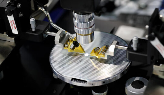
The Year in Semiconductor Device Test Feb 12, 2024 · By Mark Berry · 3D In-Depth, Test and Inspection
How is X-ray Inspection Used in Semiconductor Manufacturing? Oct 03, 2023 · By Nordson Test and Inspection · 3D In-Depth, Test and Inspection
Thermal Test Chips (TTCs) for Advanced Semiconductor Packaging Aug 16, 2023 · By Dr. Dongkai Shangguan · 3D In-Depth, Test and Inspection
An Inside Look at 3D-DfT Standard IEEE Std 1838™-2019Mar 17, 2020 · By Francoise von Trapp · 3D In-Depth
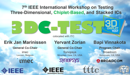
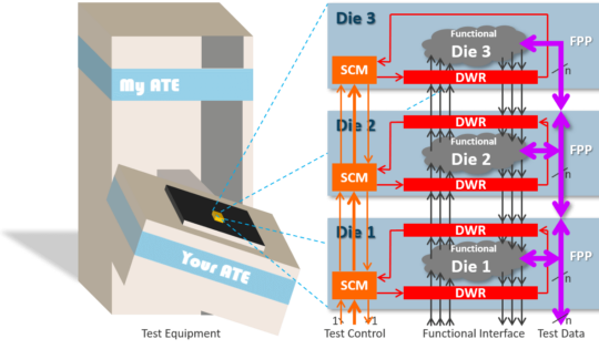
Eight years in the making, the IEEE Std 1838™-2019 Standard for Test Access Architecture for Three-Dimensional Stacked Integrated Circuits — or IEEE 1838,...
3D Test: No Longer a Bottleneck!May 17, 2019 · By Erik Jan Marinissen · 3D In-DepthWhen I joined imec in October 2008 to work on test and design- for- test (DfT) of 3D-stacked integrated circuits...
Reliable Process Control Solutions for the Growing Power Device MarketApr 11, 2019 · By Dario Alliata · 3D In-DepthThe expected increase of the power device market, with a compound annual growth rate (CAGR) of more than 10% —...
New Solution for Testing Chips Prior to 3D StackingAug 21, 2017 · By Erik Jan Marinissen · 3D In-DepthStacking chips on top of each other (aka 3D stacking) is a well-known approach to make more compact and powerful...
Executive Viewpoint: The Impact of Process Control on FOWLP and 3D ICJun 17, 2015 · By Francoise von TrappAs Si interposer and 3D stacked memory devices enter into production, albeit in low volumes, semiconductor manufacturers are lining up...
Advancing Sensing Solutions to 3D and BeyondMar 19, 2015 · By Francoise von Trapp · BlogsA second side trip on the way to DATE 2015 brought me back to Nimes, France to check up on...
Putting 3D Integration to the TestOct 29, 2014 · By Francoise von Trapp · 3D Event Coverage3D stacking is “already old hand”; or so declared Brion Keller, Cadence, in his keynote talk at last week’s 5th...
KLA Tencor: CV310i Wafer Edge Inspection and Metrology ModuleJun 23, 2014 · By Francoise von Trapp · 3D In-DepthCIRCL CV310i module is an advanced Wafer Edge inspection, metrology and profiling system tailored for Advanced Wafer Level Packaging. Simultaneous...
Fogale: TMAP DUAL 3D 300 AMay 23, 2014 · By Francoise von Trapp · 3D In-DepthThe TMAP DUAL 3D 300 A is a unique metrology and inspection tool available to the semiconductor industry capable of...
NORDSON Dage: XM8000 Wafer X-ray Metrology PlatformMay 12, 2014 · By Francoise von Trapp · 3D In-DepthFully automatic, in-line X-ray metrology platform for the measurement and defect capture of both optically hidden and visible features in...
Cascade Microtech: In the imec 3D Test LabApr 07, 2014 · By Francoise von Trapp · 3D In-DepthMy visit to imec to meet with the Cascade Micorotech and imec 3D Test collaboration team included a tour of...
Cascade Microtech Breaks Through the Barriers of 3D TestApr 07, 2014 · By Francoise von Trapp · BlogsFor quite some time, the lack of cost-effective test solutions for 2.5D interposers and 3D stacked ICs (3D SICs) has...
3D Integration Workshop Faces Reliability Challenges Head OnApr 01, 2014 · By Francoise von Trapp · 3D Event CoverageThe Friday 3D Integration Workshop at DATE 2014 once again found me among friends, as an intimate group of about...
Fogale Nanotech: Building The Swiss Army Knife of 3D IC Metrology and InspectionMar 25, 2014 · By Francoise von Trapp · BlogsIn the world of 3D ICs, where features are becoming finer and submicron accuracy and precision is more important than...
Making Progress with 3D IC Design and TestMar 07, 2014 · By Francoise von Trapp · 3D In-DepthThank you, Ann Steffora Mutschler (Semiconductor Engineering) for getting to the bottom of the difference of EDA tools for 2.5D...
Progress Reports for 3D IC Thermal Management and TestFeb 20, 2014 · By Francoise von Trapp · 3D In-DepthIn Jan Vardaman’s recent readiness report card issued at 3D ASIP in December, 3D IC thermal management issues scored and...
3D TSV Test Approaches: Outlook for 2014Jan 08, 2014 · By Bernhard Lorenz · BlogsMetrology, process control, and electrical test are key enablers for the success of the semiconductor industry. 3D integration using TSVs...
Rudolph Technologies’ Metrology, Inspection and Lithography Solutions for 2.5D and 3D TSVsNov 18, 2013 · By Francoise von Trapp · 3D Event CoverageHere’s one thing the team at Rudolph has a firm grasp on: understanding that feature sizes of today’s wafer-level, 2.5D...
Probing Questions at the IEEE 3D IC Test WorkshopSep 23, 2013 · By Francoise von Trapp · 3D Event CoverageAs this year’s 3D IC Test Workshop unfolded (September 12 & 13, 2012), one thing became increasingly clear to me:...
Multitest’s Next Phase: An Interview with Reinhart RichterSep 19, 2013 · By Francoise von Trapp · 3D In-DepthThis past July, I visited Multitest’s San Jose location to learn about the company’s activities in 3D IC test, as...