


A second side trip on the way to DATE 2015 brought me back to Nimes, France to check up on activities at Fogale Nanotech since last year. I was reminded once again, that Fogale isn’t just a semiconductor equipment supplier. Its core competencies are optical and capacitive sensing technologies, and thanks to the entrepreneurial spirit of the company’s CEO, Patrick Leteurtre, the company continues to invest in its engineering ideas, finding new applications for its sensing solutions.
Touchless Touch Screens
Last year, I caught a glimpse of one of those applications, a touchless touchscreen technology called Fogale Sensation that targets smartphone and tablet displays, as well as gaming devices. The latest cool video shows off the functionality this technology adds to smart watches. As I am one to connect the dots, it occurred to me while watching this video that this could be the perfect solution to what I see as the greatest drawback of the World Made of Glass concept: smeary screens. (Corning guys, if you’re reading this, you really need to check it out.)
Metrology for BSI
The primary reason for my visit, however, was to get an update on activities focused on metrology solutions for advanced wafer level packaging and 3D ICs.
 According to Gilles Fresquet, VP of the semiconductor division, despite the fact that the TMAP 3D Dual 300 was developed with 3D IC metrology requirements in mind, the tool, which won the 2014 3D InCites Award for the inspection and metrology tool category, is currently in demand for fan-out wafer level package applications, particularly in Asia. This is likely due to the attractiveness of these technologies to replace flip chip chip scale packages (FC-CSP) in mobile phones and tablets, while 3D IC with TSVS is still at low volumes in 3D DRAM for high-performance computing applications. For FOWLP, the tool is configured to accommodate wafer on a frame, and is set up to handle either FOWLP or interposer integration applications. Guénael Ribette noted that the TMAP can also be configured for microfluidic applications, such as ink jet print heads, and infrared focal plane arrays (IR FPAs).
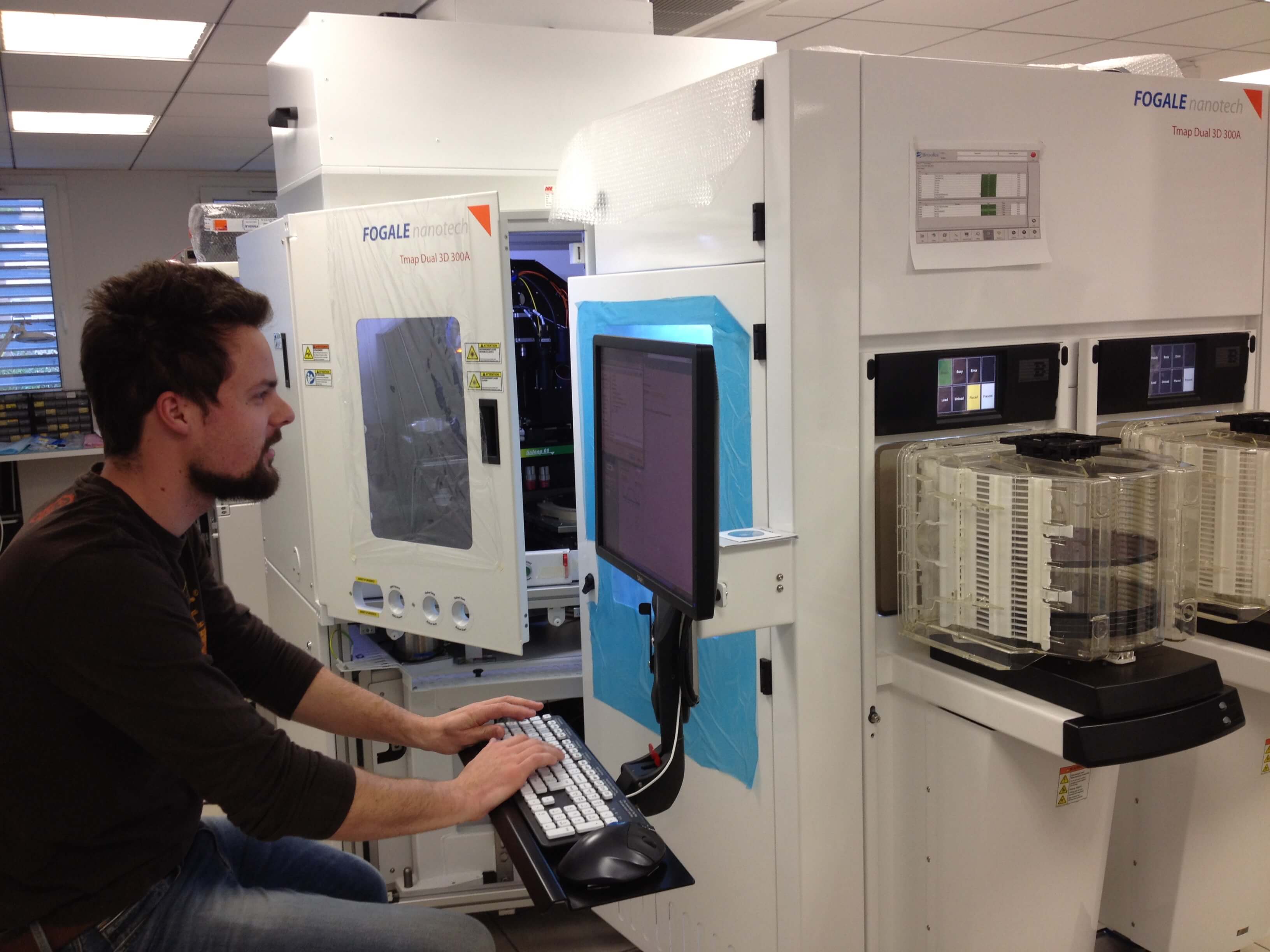 Ribette and Fresquet showed me an almost completed tool destined for installation later this month at CEA-Leti, as part of a collaborative European project with Leti, Fogale, EV Group and ST Microelectronics. The project, POLIS, which stands for Pilot Optical Line for Imaging and Sensing, is part of an initiative to grow Europe’s position in the phonic sensor technology and imaging market. Fresquet noted this was a $692M market in 2012, that is expected to grow to 2.5B by 2017.
Fogale’s work in this project, with Leti, EV Group, and ST Microelectronics, has been to provide metrology solutions for Cu-Cu bonding for backside illuminated images sensors (BIS), for which high accuracy alignment is critical.
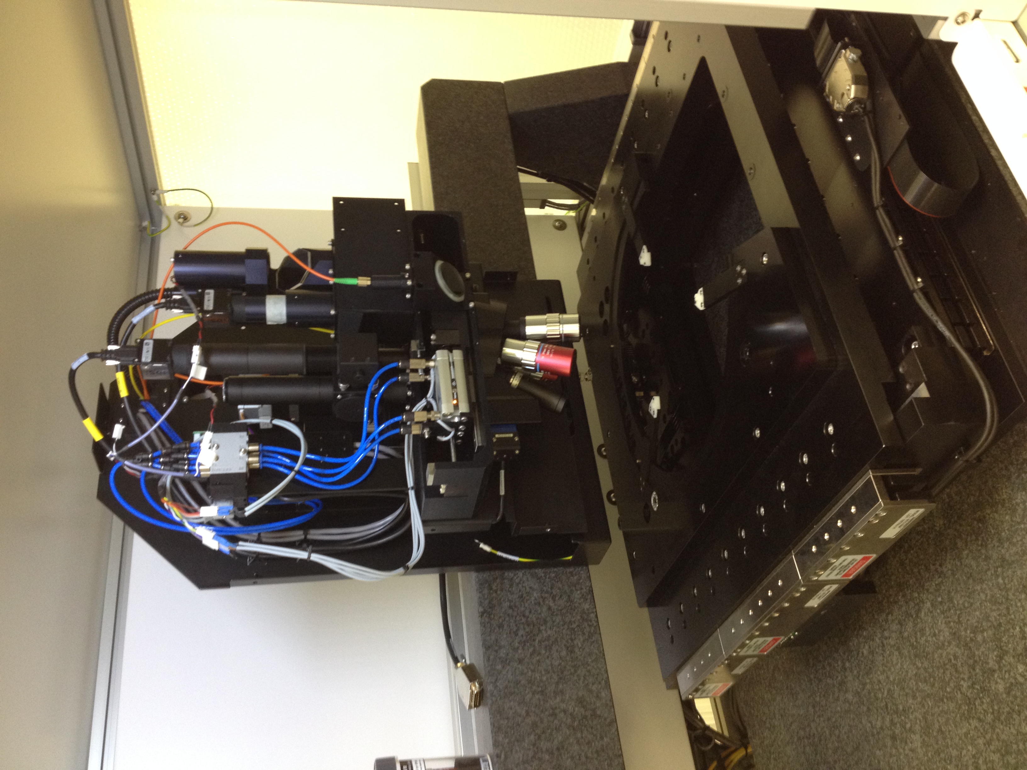 Fresquet explained that this tool is built on the TMAP Dual 3D 300 platform, but “has a new heart of the system for Cu-Cu bonding.” The dual sided configuration is made possible by an open stage that allows for <0.5µm accuracy. It features low to high field of view (FOV) microcopy technology combined with full field interferometry, and operates with proprietary signal analysis software.

Metrology for Cu-Cu bonding for BSI applications is a two-step process, explained Fresquet. First, it performs a sub-nanometer surface profile to control the CMP process just before bonding to make sure there are no artifacts from dielectric layers. It also characterizes dishing of the copper pads on the wafer. After bonding, there is a second pass through the tool for an in-plane/out-of-plane measurement with 0.1µm accuracy. The tool also allows for double sided imaging to minimize time for stitching calculations, noted Ribette. Additionally, the stage doesn’t move in the z-axis, which means the autofocus works less and saves time.
Fresquet says BSI is the first application for this particular tool configuration. He says he sees promise in future applications, because its full field of view capabilities eliminates the need to deposit and opaque layer to mask any dielectric artifacts for performing CMP measurement. Additionally, the two-step processes allows for measurement correlation before and after bonding.
Another Blade in the Victronox
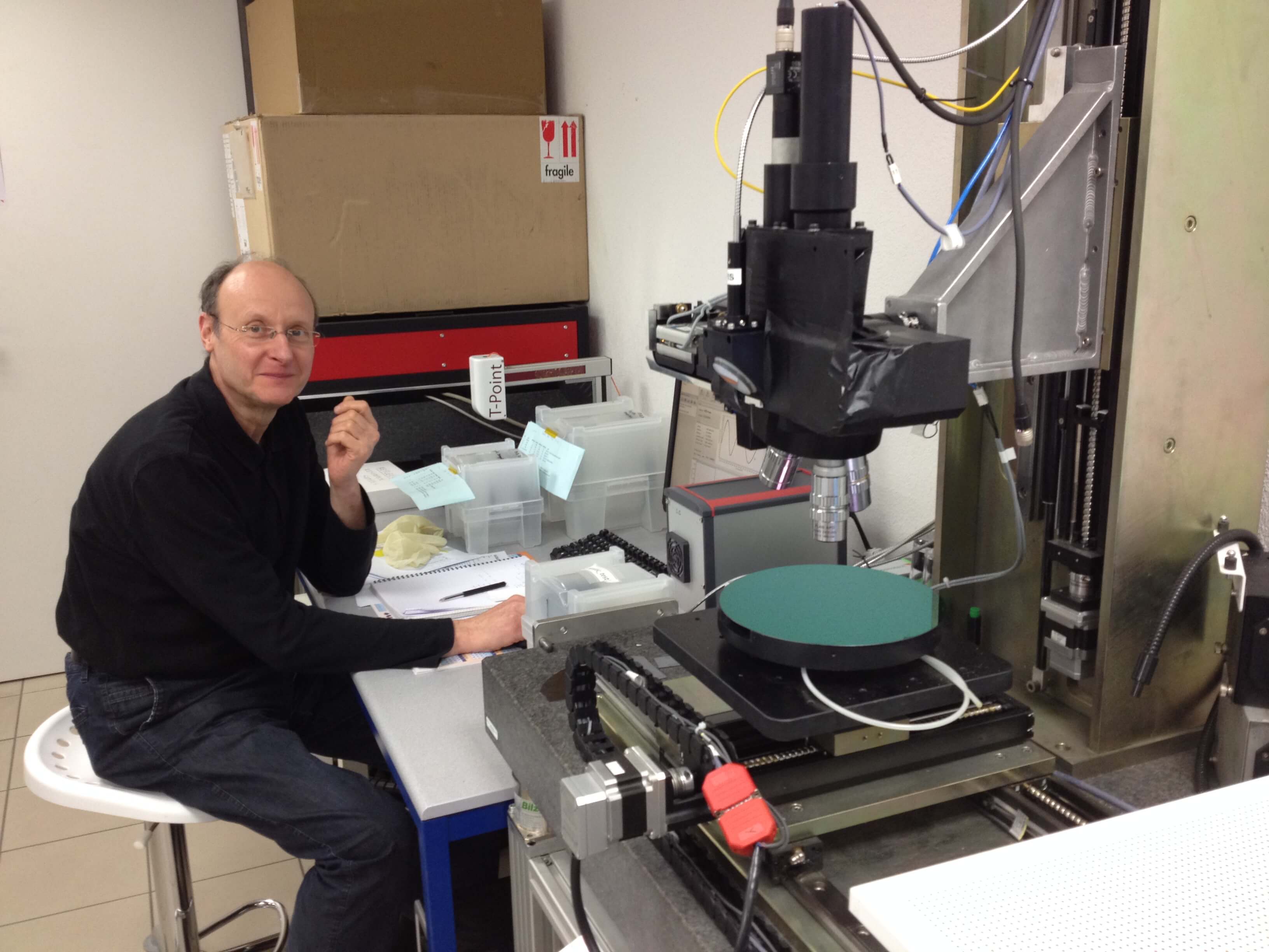 What makes the TMAP Dual 3D 300 unique in its class is that it combines microscopy techniques with a temporal-mode interferometer and a spectrometer in the same optical path. Dr. Jean-Philippe Piel, Metrology Director, has been hard at work developing a new blade for this “swiss army knife“; a reflectometry sensor to measure extremely thin film layers. Similar in concept to spectrometry, the key difference is in the mathematical treatment of the signal. “Reflectometry proposes a different model than spectrometry,” explained Piel. “In a stack of material it measures reflectivity versus wavelength.”
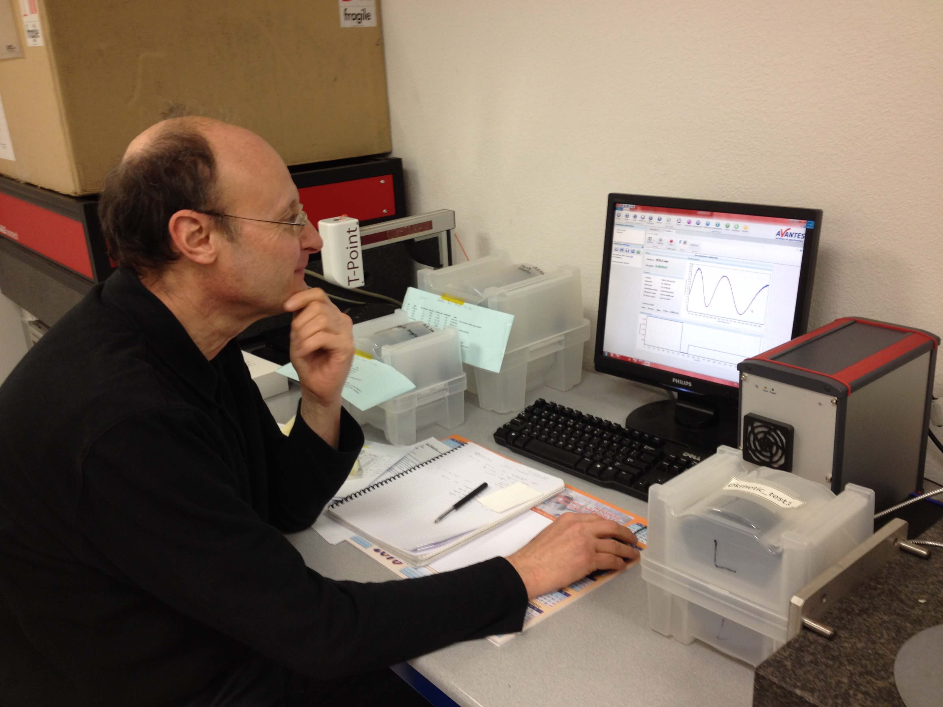 Piel demonstrated how light from a simple halogen lamp light sources source is sent to the wafer surface using an optical fiber to an objective microscope. The light is reflected and travels back through another optical fiber to the spectrometer, which analyzes light vs. wavelength.The reflected light gives information about layers deposited on the layer to explain the structure of the wafer surface. A rough surface reflects poor light, he said. Sample measurements are compared with that of a bare silicon “reference sample” which has a known reflexive index. The sample he used for demonstration had a thin oxide layer on a silicon on insulator (SOI) wafer. He said the range of measurement this new sensor technology is capable of is 500nm up to 1µm wavelength, which is the baseline measurement.
The main application for this new sensor technology will be to measure thin film between two wafers because in infrared mode, it is possible to measure through silicon. While the technology is still in development, it is destined for the production environment, said Piel, and will add complexity to the TMAP. ~ F.v.T.


