
If you love, like me, to work on the bleeding edge of technology, you will find that your personal success depends very much on the team around you, your company, even the entire supply chain. The organizers of this workshop – AMD’s Michael Alonso, Advantest’s Dave Armstrong, and MEPTEC’s Ira Feldman – clearly recognize this important fact and engaged experts across the entire supply chain (see Figure 1) to address KGD in a very holistic manner.
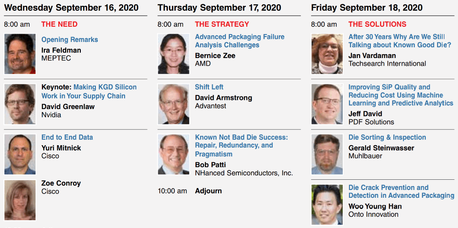
In two-hour blocks, on September 16 – 18, the speakers addressed many important KGD topics from their perspectives. This webinar series was free to attendees thanks to these corporate sponsors: ASE Group, ADVANTEST, Gel-Pak, Muhlbauer, HighTech International, Amkor Technology, and MicroCircuit Laboratories.
System Vendors Express Needs
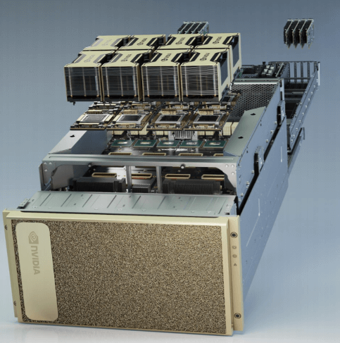
After a brief intro by Ira Feldman, David Greenlaw, VP Product Engineering at Nvidia, described in-depth how market demand for cost-effective and power-efficient computing resources is growing exponentially. He stated that the 1000 X performance enhancements during the last ten years have been achieved by improving silicon, packaging, and software. Greenlaw described their latest N100 card. It is comprised of a large multi-instance GPU with 54 Billion transistors in TSMC’s 7 nm process and six HBM2 memory stacks, offering a bandwidth of 1.6 Terabyte/sec. Eight of these cards, a Dual 64-core AMD Rome CPU, one Terabyte of RAM, six NVSwitches, and nine Mellanox interface cards build the core of Nvidia’s DGX A 100, third-generation integrated AI system, priced at $199,000.
After this impressive excursion into the high-performance systems world, Greenlaw focused on his supply chain. He highlighted two weaknesses in the current KGD and advanced packaging assembly world: Internally, OSATs need to adopt a more wafer-fab-like working culture, e.g. practice statistical process control (SPC), failure mode, and effects analysis (FMEA), and strive for continuous improvements. Externally, they need to adopt a wafer-fab-like service mind set and treat their customers like partners.
To soften his comments, he reminded the audience how wafer foundries and DRAM suppliers had to mature on their way to big business success. Greenlaw pointed out that customer focus means:
- See your customer’s success as key to your own success
- Own the whole problem; drive to closure
- Listen to your own customer support teams
- Realize that solving customers’ problems is a key ingredient for every engineer’s personal success and essential for the success of his/her team and company.
In response to questions, Greenlaw replied: Strengthening the customer engineering function and intensifying dialogs with customers will improve OSATs’ margins. Establishing unit-level traceability will reduce debug time, improve yields, and accelerate production ramp-up.
Cisco’s Perspective of KGD
Zoë Conroy from Cisco’s Quality and Technology Department started with an important point: A KGD on the tester can turn bad in a real system environment. She explained system assembly and test, then highlighted what component vendors need to consider to anticipate the impact of noise, power & signal integrity, temperature cycling, and interactions with other components before a die can be declared KGD in an end-to-end (ETE) system context. Her colleague, Yuri Mitnick, emphasized that the “known-good” concept also applies to modules, subsystems, and systems and requires the responsible engineering teams to work together in the test, debug, and repair activities.
Strategies for Test, Debug, and Repair
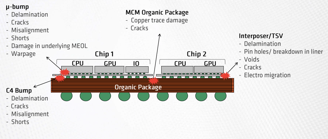
Bernize Zee at AMD in Singapore explained the importance of failure analysis (FA) and how/where the rapidly increasing complexity and heterogeneous functionality in multi-die packages bring new FA challenges (Figure 3). Zee outlined a number of FA projects and described how she used different analysis techniques to identify failures and recommend corrective actions.
Dave Armstrong from Advantest titled his presentation “shift left” but also mentioned that some test steps trend to shift right, e.g. performing logic level tests at the system level test (SLT) stage. Then he showed in several different ways why catching failures early makes sense and lowers cost. He substantiated with cost comparisons that, especially when combining several large dice in a package, the savings of the shift-left strategy, e.g. exhaustive wafer and die testing, are significant and improve KGD quality and margins.
Bob Patti from NHanced Semiconductors prefers to call KGD “Known Not Bad Die” and discussed the value of repair, redundancy, and pragmatism. He emphasized that component failures in IoT networks with billions of nodes, in automotive and other applications, can be very costly. Therefore, he suggests adding redundancy and designing for repair where the additional cost is practical. He gave some redundancy examples, e.g. spare processors in multi-core CPUs, smart interposer to re-route signals, redundant I/Os, etc.
Solutions that Contribute to High-Quality KGD
Jan Vardaman, Founder, and President of TechSearch International confirmed that 30+ years ago, when she started her company, KGD was already an important discussion topic. How much progress have we made since? She confirmed that built-in self-test (BIST) and redundancy play important roles now, the latter especially in memories and interconnects between chiplets because multi-die assemblies are impossible to repair. Then she showed how several industry leaders design their multi-die ICs to achieve high quality and reliability. You can view her entire presentation here:

Jeff David, from PDF Solutions, outlined how machine learning (ML) and predictive analytics can improve product quality. He warned that chiplets, like fully packaged ICs, can include hardware trojans, therefore need to be tested thoroughly. ML helps to untangle complex relationships and to spot failures faster than traditional FA methods. David showed several examples where PDF’s ExensioR engine predicted failures, improved product quality, and ramp-up time.
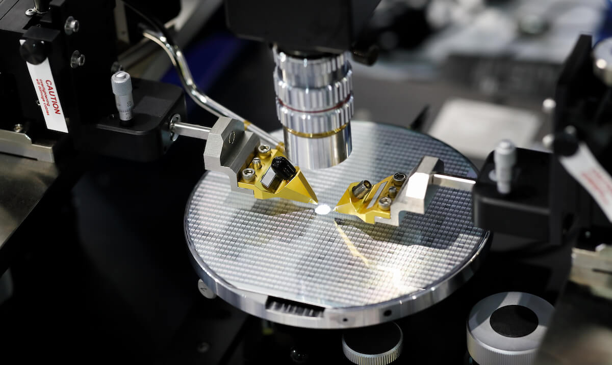
Gerald Steinwasser from Muhlbauer talked about their equipment’s capabilities to inspect die visually for cracks, particles, and other defects, using regular and/or infrared light. He, like other speakers, also emphasized the importance of traceability, to locate root causes of failures quickly.
Woo Young Han from Onto Innovation, the combination of Nanometrics and Rudolph Technologies, focused his talk on how to prevent and detect different types of die cracks (Figure 4).
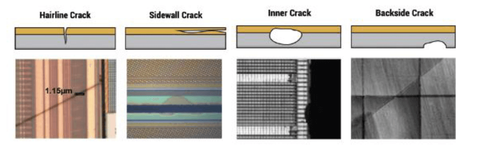
As die thicknesses down to 50µm are becoming more common, the fragility of such dice demands caution during separation and beyond the regular test steps, additional inspections to avoid reliability problems. He mentioned that even laser cutting can cause a crack and justifies such additional die inspections. You can view his entire presentation below:
Personal Comments
Having been on the bleeding edge of CMOS logic, FPGAs and ASICs, emerging foundries, EDA tools and advanced IC packaging, I fully endorse Greenlaw’s call for closer customer-supplier relationships. Only good personal management and engineering relationships and customer-friendly support organizations, e.g. design centers, can enable the vast amount of mutual learning that is necessary to make a bleeding edge technology successful. I have seen many companies with great products bleeding to death, before having established strong partnerships with teaching customers.
I am glad that major OSATs are now developing, jointly with customers and mutual EDA partners, Package Assembly Design Kits (PADKs). Just like PDKs accelerated the growth of the fabless – foundry business model, PADKs will enable OSATs to be proactive, engage customers faster and guide them to cost-effective and reliable packaging solutions. In addition, PADKs will establish a data exchange mechanism that will accelerate learning on both sides.
If you want to know more about these useful presentations, all slides can be downloaded from MEPTEC’s website and you can enjoy any one or all presentations at MEPTEC’s YouTube channel. ~ Herb


