 When I joined imec in October 2008 to work on test and design- for- test (DfT) of 3D-stacked integrated circuits (ICs), there were only a few test folks active in that emerging field. Consequently, misconceptions about 3D test were omnipresent. In the November 18, 2008 issue of Semiconductor International, Alexander Braun wrote: “At a symposium yesterday on 3-D integration, leading expert Philip Garrou detailed the rise of the technology as well as the challenges facing it, including test, yield, and design. (…) Test, again, will be a significant problem. Memory can be stacked as known good die because the memory chips can be tested, but years from now, as different functions are pulled apart to stack them, there is no clear way to test them because they do not form a complete circuit. This will hold up things like the full partitioning of chips.”1 3DInCites’ tenth anniversary is a good occasion to report on the state of 3D testing and publicly declare it no longer a bottleneck for 3D integration.
Structural Modular Test
‘Test’ is an overloaded term. While some people might think of design verification (on a simulation model) or design validation (on the real chip), this article is restricted to electrical testing for manufacturing defects, typically in a high-volume setting. At this stage of product development, we assume chip designs are correct. Chip manufacturing processes are defect prone as they consist of large numbers of high-precision steps. Unavoidably things go wrong every now and then, leading to spot defects such as shorts and opens.
For a large chip manufactured using advanced technology, the die yield might be 80%, while customers typically tolerate defective chips in quantities of no more than100 defective parts per million (dppm). Consequently, a test needs to be a very effective filter for defective chips. Because every transistor or interconnect segment on a chip can suffer from defects, each chip needs to be tested, and hence the test needs to be very efficient; taking no more than a few seconds per chip in a fully automated process.
During test, stimuli are fed into the chip and corresponding responses on the chip outputs are compared to expected responses to determine ‘pass’ or ‘fail’. Automatic test pattern generation (ATPG) tools, available from all major EDA suppliers, try to cover as many potential fault locations as possible with a minimum of test patterns to reduce test time and associated cost.
ATPG tools do not utilize application knowledge of the device-under-test (DUT), but instead, base themselves on the DUT’s structure: the gate-level netlist with interconnected library-cell instances (AND, OR, flip-flop, etc.). The resulting test patterns have no relation with the mission-mode (‘functional’) operation of the chip, but check if these cells are present, operational, and correctly interconnected. We refer to this as a structural test (as opposed to a functional test).
For a structural test, testing a single die that only implements a partial function of a multi-die stack is no problem at all. This modular approach to test development and execution has become a common practice in the industry. Today’s core-based system-on-chips (SOCs) are routinely tested in a modular fashion: core-by-core, sequentially, or all at the same time.2
For 3D integrated circuits (3D ICs), for which the various stacked dies might be designed and/or manufactured by different parties, modular testing (here: die-by-die) makes even more sense. The benefits include:
- Targeted test pattern generation, tailored to the circuit type (e.g., logic or memory) and function, preferably by the team also responsible for the design
- Freedom to (re-)schedule the various die tests if manufacturing yields so require (test engineers like to put tests that are more likely to fail early in their test suite, to reduce the per-die average test time by applying ‘abort-on-fail’)
- Re-use of tests in case design modules are reused
- First-order fault diagnosis and yield attribution (because: if the test for a particular module fails, that module most likely contains the root cause)
Test Flow Optimization
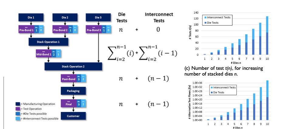
A major difference between testing 2D and 3D ICs is the potential complexity of the test flow. At which moments in the manufacturing flow do we execute a test for what stack component? Conventional 2D chips typically have two test moments: first while still in their wafer (wafer test, a.k.a. e-sort), to avoid package costs for defective dies, and then again after assembly and packaging (final test), to guarantee the outgoing product quality toward the customer. 3D ICs have many more test moments, tests, and hence test flows. For an n-die stack, we have prior to stack assembly n possible test moments during which we can execute a pre-bond test on a die. After every stack assembly operation, we have a new test moment, in which each die and interconnect layer in the stack built up so far can be tested. We refer to these test moments as mid-bond tests (for partial stacks) and post-bond tests (for complete stacks). There are ∑ n i=2 (i) die tests and ∑ n i=2 (i-1) interconnect tests possible during these test moments. After packaging, the final test can contain n die tests and (n-1) interconnect tests. In total, an n-die stack has 2n test moments during which a grand total of 2n-1+ ∑ n i=2(i) die tests and n-1+∑ n i=2 (i-1) interconnect tests might occur. In practice, there might be no physical test access during certain test moments, which reduces the number of feasible tests. A test flow consists of an execution decision (yes/no) for each test at each feasible test moment. If a die stack has a total of t(n) tests, this allows for f(n)= 2t(n) alternative test flows. Note: this definition of f(n) does not account for alternative test schedules due to reordering of tests at a particular test moment.
Figure 1(a) illustrates the test flows for a relatively simple stack with only three dies, resulting in 16 tests (11 die + 5 interconnect tests), and therefore a total of 216 = 65,536 alternative test flows. In practice, some test moments might not permit probe access, and this reduces the number of feasible tests and test flows. For example, for imec’s FC-FOWLP test chip consisting of seven dies, from the theoretical 68 tests only 33 tests are practically feasible; which still implies a whopping 233 » 8.6´109 alternative test flows. Figure 1(b) shows the generic equations for t(n) as a function of the number of stacked dies n. Figures 1(c) and 1(d) depict t(n) respectively f(n) as a function of the number of stacked dies n.3
The large numbers of alternative test flows necessitate computer support. The 3D-Costar software tool, developed by TU Delft and imec, makes a cost analysis of user-specified manufacturing and test flow.4 The tool considers costs proper to design, as well as five manufacturing operations:
- Wafer processing
- Stack assembly
- Test
- Packaging
- Logistics
These operations are considered not perfect and are modeled with an associated yield (in percent). For test, ‘yield’ is defined as 100% minus the test escape rate (in dppm). 3D-Costar calculates the lump-sum costs per operation, where all costs are attributed to those stacks that pass the entire flow and are indeed shipped to the customer. The tool can analyze the effect of varying an arbitrary number of parameters (in lock-step) along one or two independent axes, as variations of a user-defined base case. The output of the analyses is an estimation of product quality (defective chips that nevertheless pass the test, in dppm) and the cost per shipped stack, sub-divided over the subsequent manufacturing operations.
Test Access
The main challenges of 3D testing are all related to test access: delivering test stimuli to where they actually can detect the presence of a defect, and the test responses in the opposite direction. Test access has two components: external test access, i.e., from the test equipment to the chip I/Os and back, and internal test access, i.e., from the chip inputs to the actual on-die defect location and back to the chip outputs.
With external test access, several challenges and their solutions related to probing on ‘naked’ (not-yet-packaged) dies or die stacks are described below. Internal test access is handled by on-chip DfT hardware. The conventional (‘2D’) DfT has been extended with 3D-specific features, and those are described at the end of this article.
Probing Challenges and Solutions
For most product scenarios, realistic yields require a combination of pre-, mid-, and post-bond testing. This prevents manufacturing defects from being discovered too late in the stack-assembly flow thus requiring the entire stack to be scrapped, including perhaps other (defect-free) dies. Whereas test access contact for final test is made through a test socket, the pre-, mid-, and post-bond tests all depend on probe technology. For multi-die stacks, the following probing challenges have been identified and resolved in collaboration with our partners.5
Probing on large tape frames
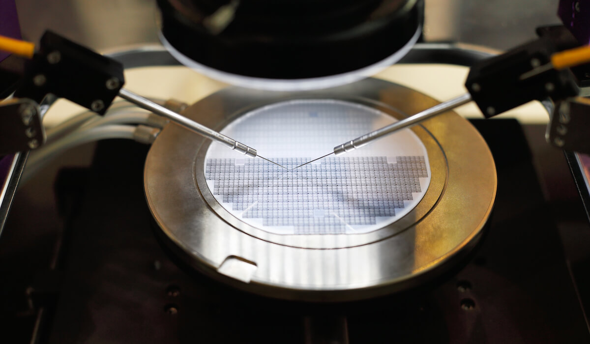
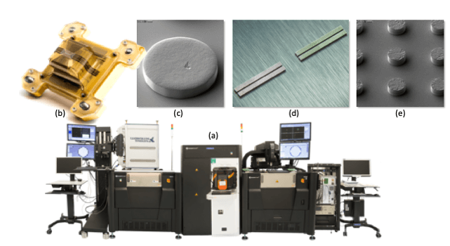
Stack-assembly flows for multi-die stacks frequently use tape frames as a temporary carrier: for diced wafers, for aggressively thinned-down wafers, for pick-n-placed dies and die stacks, etc.6 Out of necessity, a tape frame is larger than the wafer it holds; for a ø300mm wafer, the outer dimension of the frame is ø400mm.7
Imec worked with Cascade Microtech (now FormFactor) to specify and implement adaptations to the CM300 probe station, so that ø300mm wafers on a large tape frame can be loaded manually.6 The Tokyo Electron WDF-12DP probe station even has an automatic loader for such large tape frames.8 (Figure 2)
Probing ultra-thin wafers on a flexible tape
Wafer thinning is commonly performed on dies used in multi-die stacks: from 780µm down to ~200µm to fit the stacked dies into a standard-height package cavity or, when TSVs are employed, even thinner to expose the TSVs at the wafer back-side (at imec: 50µm). Stretched UV-curable dicing tape, laminated over a tape frame, is commonly used as a temporary carrier to prevent ultra-thin wafers from sagging and curling. The forces exercised by probe needles should be sufficiently high to guarantee an acceptable low contact resistance between each probe tip and its corresponding probe pad. However, when we do this on an ultra-thin and flexible wafer atop of a flexible and stretchable dicing tape, we should avoid probe forces that cause permanent or even temporary stress-induced electrical or mechanical effects and damages. At imec, we have done numerous experiments with probe cards that require different probe forces: conventional cantilever, FormFactor’s Pyramid®, and Pyramid® RBI (Rocking Beam Interposer) MEMS-type probe cards, and Technoprobe’s ARIANNE™ and TPEG™ probe cards. We recommend a low-force probe card in this situation.
Probing large arrays of fine-pitch micro-bumps
The interconnect between stacked dies consists of large arrays (>1,000) of Cu and Sn micro-bumps at ultra-fine pitch: 40µm. Imec has developed a unique test system to characterize probe cards that claim to be capable of probing such micro-bump arrays [9]. It consists of a FormFactor CM300 probe station with hard-docking National Instruments test head with 1,216 parametric tester channels.9 Imec has in-house manufactured test wafers with only micro-bumps (>10 million micro-bumps at 40µm pitch on a ø300mm wafer) in various metallurgies. This set-up has been successfully used to characterize advanced micro-bump probe cards which imec co-developed with leading suppliers: FormFactor’s Pyramid® RBI and Technoprobe’s TPEG™ T40.10, 11
Probing singulated dies and die stacks on a flexible tape.
The challenge is that the probe targets might have translated or rotated from their original wafer-map position, such that blind index stepping by the probe station is no longer possible. This happens when probing on diced wafers or diced stacks on dicing tape, due to the flex-n-stretch forces of the dicing tape). Another application is pick-and-place of die-to-die stacks on a carrier substrate, as the pick-and-place tool might be insufficiently accurate for subsequent probing.8 Together with our partner FormFactor, we have developed and successfully demonstrated software that determines the individual misalignment per die or die stack at the start of the wafer probe session and then compensates for it while probing.8

Originally deemed impossible when we started to work on this topic in 2011, today imec is probing 40µm-pitch micro-bump arrays on a routine basis. Recently, we reported on a case study where all probing challenges described above and their proposed solutions, were applied in a combined fashion.5
3D-Design-for-Test Architecture
For transportation of stimuli and responses within the die (stack), we need on-chip DfT. Conventional 2D-DfT includes internal scan chains, test data compression to handle large dies, core-test wrappers around embedded cores and other design units that will be tested as stand-alone units, and built-in self-test hardware for embedded memories. With the term ‘3D-DfT’ we refer to on-chip DfT features that are explicitly added to handle 3D ICs.
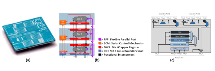
A 3D-DfT architecture should support a per-die modular test approach and therefore requires wrappers at die level, such that the various dies and their inter-die interconnects can be tested independently from each other. Whereas conventional 2D core wrappers (as specified by IEEE Std 150012) have one test input and one test output port, a 3D-DfT die wrapper should support multiple test ports. A die has its test data to and from the test equipment enter and exit via its primary test port. In case one or multiple other dies are stacked directly on this die, it will also have a corresponding number of secondary test ports, which each serves as a plug for the primary test ports of one of these stacked dies. In this way, test stimuli can enter the stack through the primary test port of the base die, be transported up in the stack, possibly through other dies, to reach the destination die where they execute their defect detection work; likewise, test responses need to be transported from the DUT through other dies in the stack down to the external stack I/Os.
Imec defined and patented a 3D-DfT architecture that meets these requirements, initially for single-tower logic-on-logic die stacks (Figure 3). With Cadence Design Systems we developed an EDA tool flow for DfT insertion and test generation EDA tool flow; and we designed, manufactured (partly at GlobalFoundries, partly at imec), and tested successfully a demonstrator IC containing the proposed 3D-DfT.13, 14
3D-DfT Standardized: IEEE Std P1838
To guarantee interoperability of the 3D-DfT architecture across the various dies in a stack, especially if these dies are designed by different teams or companies, a standardization effort was needed. This was done under the umbrella of IEEE Standards Association, as other DfT standards reside there as well.
In 2011, I founded a standardization working group under IEEE sequence number P1838. Standardization is intrinsically a slow process, but after eight years, the draft standard is finally nearing completion. At the end of 2018, the ballot group has been formed and in 2019 the actual ballot will take place, hopefully leading to an approved standard still in the same year. IEEE Std P1838 standardizes per-die 3D-DfT features, such that if compliant dies are brought together in a die stack, a basic minimum of cooperative test access is guaranteed to work across the stack. 19
IEEE Std P1838 consists of three main components: a die wrapper register (DWR), a serial control mechanism (SCM), and a flexible parallel port (FPP). DWR and SCM are 3D extensions of existing standards IEEE Std 1500 and IEEE Std 1149.1, respectively. The FPP, a novel feature of P1838, is an optional, scalable multi-bit (‘parallel’) test access mechanism that offers higher bandwidth compared to the one-bit (‘serial’) mandatory part of P1838. 20
Conclusion
DfT and test engineers know the limits of their work. Our industry is not making chips because the test community has developed a fancy test solution for them; customers would not care. They are interested in more performance, more storage capacity, and higher bandwidth, benefits which can be achieved with 3D ICs. But, on the other hand, our industry cannot put high volumes of products with wonderful new performance/storage/bandwidth features on the market, if these products are not individually tested for defects. Customers do not accept that.
The mere fact that the test community started working on 3D ICs was a clear sign that the release of actual 3D products was imminent. With the solutions described in this article, most of the test challenges related to 3D ICs have been addressed, such that we can conclude that ‘test’ is no longer a bottleneck for the market introduction of 3D ICs. The test community has delivered, adequately and, while the first products are hitting the market right on time!
If you want to read more about 3D (test) challenges and solutions: they are described in detail in the book “Design, Test, and Thermal Management”, edited by Paul D. Franzon (NCSU), Erik Jan Marinissen (imec), and Muhannad S. Bakir (Georgia Institute of Technology). This book is Volume 4 in the well-known book series “Handbook of 3D Integration”, published by Wiley-VCH and available from March 2019 onward.
Editor’s Note: This article first appeared in 3D InCites: The First Decade. Download the issue here.
About the Author
Erik Jan Marinissen is a principal scientist at imec in Leuven, Belgium, the world-leading independent R&D center in nanoelectronics technology. His research on IC test and design-for-test cover topics as diverse as 3D-stacked ICs, CMOS below 10nm, silicon photonics, and STT-MRAMs. Marinissen is also a visiting researcher at the Eindhoven University of Technology in the Netherlands. Previously, Marinissen worked at NXP Semiconductors and Philips Research in Eindhoven, Nijmegen, and Sunnyvale. Marinissen is (co-)author of 250+ journal and conference papers (h-index: 43) and (co-)inventor of 18 patent families. He has received numerous awards for his work and is very involved in IEEE conferences and standards. Among them, he served as editor-in-chief of IEEE Std 1500 and as founder/chair (currently vice-chair) of the IEEE Std P1838 Working Group on 3D-SIC test access.
References
- Alexander Braun, ‘3-D Integration Lacking in Design and Test Support’, Semiconductor International, November 18, 2008
- Erik Jan Marinissen and Yervant Zorian, ‘IEEE 1500 Enables Modular SOC Testing’’, IEEE Design & Test of Computers, Special Issue on ‘IEEE Std 1500 and Its Usage’, Volume 26, No. 1 (January/February 2009), pp. 8-17, DOI 1109/MDT.2009.12
- Arnita Podpod, Dimitrios Velenis, Alain Phommahaxay, Pieter Bex, Ferenc Fodor, Erik Jan Marinissen, Kenneth June Rebibis, Andy Miller, Gerald Beyer, and Eric Beyne, ‘High Density and High Bandwidth Chip-to-Chip Connections with 20µm Pitch Flip-Chip on Fan-Out Wafer Level Package’, Wafer-Level Packaging Conference (IWLPC’18), San Jose, CA, USA, October 2018, DOI 10.23919/IWLPC.2018.8573262
- Mottaqiallah Taouil, Said Hamdioui, Erik Jan Marinissen, Sudipta Bhawmik, ‘Using 3D-COSTAR for 2.5D Test Cost Optimization’, IEEE International 3D Systems Integration Conference (3DIC’13),
San Francisco, CA, USA, October 2013, pp 1-8, DOI 10.1109/3DIC.2013.6702351 - Erik Jan Marinissen, Ferenc Fodor, Arnita Podpod, Michele Stucchi, Yu-Rong Jian, and Cheng-Wen Wu, ‘Solutions to Multiple Probing Challenges for Test Access to Multi-Die Stacked Integrated Circuits’, IEEE International Test Conference (ITC’18), Phoenix, AZ, USA, October 2018
- Erik Jan Marinissen, Bart De Wachter, Teng Wang, Jens Fiedler, Jörg Kiesewetter, and Karsten Stoll, ‘Automated Testing of Bare Die-to-Die Stacks’, IEEE International Test Conference (ITC’15), Anaheim, CA, USA, October 2015, Paper 20.2, DOI 1109/TEST.2015.7342412
- SEMI G74-0669 Specification for Tape Frame for 300mm Wafers. Semiconductor Equipment and Materials International, San Jose, CA, USA, May 1999
- Tokyo Electron Notification, ‘Tokyo Electron (TEL) Introduces a Dual Purpose 300mm Dicing Frame Prober’, November 2008 (see http://www.tel.com/news/topics/2008/20081104_001.html)
- Erik Jan Marinissen Ferenc Fodor, Bart De Wachter, Jörg Kiesewetter, Eric Hill, and Ken Smith. ‘A Fully Automatic Test System for Characterizing Large-Array Fine-Pitch Micro-Bump Probe Cards’. In Proc. IEEE International Test Conference Asia (ITC-Asia), September 2017, DOI 1109/ITC-ASIA.2017.8097130
- Erik Jan Marinissen, Ferenc Fodor, Bart De Wachter, Jörg Kiesewetter, Ken Smith, and Eric Hill,
‘Evaluation of Advanced Probe Cards for Large-Array Fine-Pitch Micro-Bumps’, Chip Scale Review magazine, Volume 21, No. 6 (December 2017), pp. 16-20 (see http://fbs.advantageinc.com/chipscale/nov-dec_2017/#18) - Ferenc Fodor, Erik Jan Marinissen, Daniele Acconcia, and Raffaele Vallauri, ‘Leading-Edge Wide-I/O2 Memory Probing Challenges: TPEG MEMS Solution’, Semiconductor Wafer Test Workshop (SWTW’18), San Diego, CA, USA, June 2018, Paper 2.3 (see http://www.swtest.org/swtw_library/2018proc/PDF/S02_03_Fodor_SWTW2018.pdf)
- IEEE Standards Association. IEEE Std 1500™-2005, IEEE Standard Testability Method for Embedded Core-based Integrated Circuits. IEEE, August 2005, DOI 1109/IEEESTD.2005.96465
- Cadence/imec joint press release, ‘Imec and Cadence Deliver Automated Solution for Testing 3D Stacked ICs’, June 6, 2011 (see https://www.cadence.com/content/cadence-www/global/en_US/home/company/newsroom/press-releases/pr/2011/imecandcadencedeliverautomatedsolutionfortesting3dstackedics.html)
- Erik Jan Marinissen, Bart De Wachter, Stephen O’Loughlin, Sergej Deutsch, Christos Papameletis, Tobias Burgherr, ‘Vesuvius-3D: A 3D-DfT Demonstrator’, IEEE International Test Conference (ITC’14), Seattle, WA, USA, October 2014, Paper 20.2, DOI 1109/TEST.2014.7035332
- Sergej Deutsch, Brion Keller, Vivek Chickermane, Subhasish Mukherjee, Navdeep Sood, Sandeep K. Goel, Ji-Jan Chen, Ashok Mehta, Frank Lee, and Erik Jan Marinissen, ‘DfT Architecture and ATPG for Interconnect Tests of JEDEC Wide-IO Memory-on-Logic Die Stacks’, IEEE International Test Conference (ITC’12), Anaheim, CA, USA, November 2012, DOI 1109/TEST.2012.6401569
- Christos Papameletis, Brion Keller, Vivek Chickermane, Said Hamdioui, and Erik Jan Marinissen, ‘A DfT Architecture and Tool Flow for 3D-SICs with Test Data Compression, Embedded Cores, and Multiple Towers’, IEEE Design & Test, Volume 32, No. 4 (July/August 2015), pp. 40-48, DOI 1109/MDAT.2015.2424422
- Konstantin Shibin, Vivek Chickermane, Brion Keller, Christos Papameletis, and Erik Jan Marinissen, ‘At-Speed Testing of Inter-Die Connections of 3D-SICs in the Presence of Shore Logic’, IEEE Asian Test Symposium (ATS’15), Mumbai, India, November 2015, pp. 79-84, DOI 1109/ATS.2015.21
- Leonidas Katselas, Alkis Hatzopoulos, Hailong Jiao, Christos Papameletis, and Erik Jan Marinissen,
‘On-Chip Toggle Generators to Provide Realistic Conditions during Test of Digital 2D-SoCs and 3D-SICs’, IEEE International Test Conference (ITC’18), Phoenix, AZ, USA, October 2018 - Erik Jan Marinissen, Teresa McLaurin, Hailong Jiao, ‘IEEE Std P1838: DfT Standard-under-Development for 2.5D-, 3D-, and 5.5D-SIC’, IEEE European Test Symposium (ETS’16), Amsterdam, the Netherlands, May 2016, DOI 1109/ETS.2016.7519330
- Yu Li, Ming Shao, Hailong Jiao, Adam Cron, Sandeep Bhatia, and Erik Jan Marinissen, ‘IEEE Std P1838’s Flexible Parallel Port and its Specification with Google’s Protocol Buffers’, IEEE European Test Symposium (ETS’18), Bremen, Germany, May 2018, DOI 1109/ETS.2018.8400690
Acknowledgments
I thank many colleagues and partners for their fruitful cooperation: Alkis Hatzopoulos, Leonidas Katselas (Aristotle Univ. of Thessaloniki), Teresa McLaurin (Arm), Vivek Chickermane, Brion Keller, Christos Papameletis (Cadence Design Systems), Tobias Burgherr (FHNW), Eric Hill, Jörg Kiesewetter, Ken Smith (FormFactor), Sandeep Bhatia (Google), Pieter Bex, Eric Beyne, Bart De Wachter, Ferenc Fodor, Mario Konijnenburg, Arnita Podpod, Michele Stucchi (imec), Yu Li, Ming Shao (KU Leuven), Chun-Chuan Chi (NTHU), Adam Cron (Synopsys), Daniele Acconcia, Raffaele Vallauri (Technoprobe), Paul Mooney, Eric Pradel, Yoichi Shimizu (Tokyo Electron), Sandeep K. Goel (TSMC), Sergej Deutsch (TU Braunschweig), Said Hamdioui, Motta Taouil, Jouke Verbree (TU Delft), Hailong Jiao (TU Eindhoven), Konstantin Shibin (TU Tallinn), and Michael Wahl (Univ. Siegen)
Part of this work was performed in the project ESiP, ‘Efficient Silicon Multi-Chip System-in-Package Integration – Reliability, Failure Analysis and Test’, funded by the ENIAC Joint Undertaking (http://www.eniac.eu). This project was the winner of the ENIAC Innovation Award 2013. Part of this work was performed in the project SEA4KET, ‘Semiconductor Equipment Assessment for Key-Enabling Technologies’ (http://www.sea4ket.eu), sub-project 3DIMS, 3D Integrated Measurement System, which received funding from the European Union’s Seventh Programme for research, technological development, and demonstration under grant agreement No. IST-611332.
Awards Related to This Work
- Erik Jan Marinissen received the Meritorious Service Award from the Test Technology Technical Council of IEEE Computer Society “for significant services as Program Chair of the IEEE International Workshop on Testing Three-Dimensional Stacked ICs (3D-TEST) since 2010”.
- Mottaqiallah Taouil, Said Hamdioui, and Erik Jan Marinissen received the Technology Transfer Award 2015 from HiPEAC for the 3D-COSTAR Test Flow Optimization Tool (https://www.hipeac.net/news/6774/hipeac-tech-transfer-award-2015-winners-announced/).
- Imec received the Research Institute of the Year 2017 award from 3DInCites (https://www.3dincites.com/3d-incites-awards/2017-3d-incites-awards-winners/).
- Ferenc Fodor, Bart De Wachter, Erik Jan Marinissen, Jörg Kiesewetter, and Ken Smith received the Engineering Impact Award 2017 from National Instruments in the category Electronics and Semiconductors for large-array fine-pitch micro-bump probing (https://forums.ni.com/t5/NI-Blog/Changing-the-World-with-Science-and-Engineering-2017-Engineering/ba-p/3615313).
- Erik Jan Marinissen received the Emerging Technology Award 2017 from the IEEE Standards Association “for his passion and initiative supporting the creation of a 3D Test Standard” (https://standards.ieee.org/about/awards/etech).