Henkel News

The Telecom Network Semiconductor Trifecta
Telecommunication networks are undergoing a rapid transformation. With 5G rollouts, edge computing, and a surge in IoT devices, the pressure...
An Inside-out-view: Data Centers
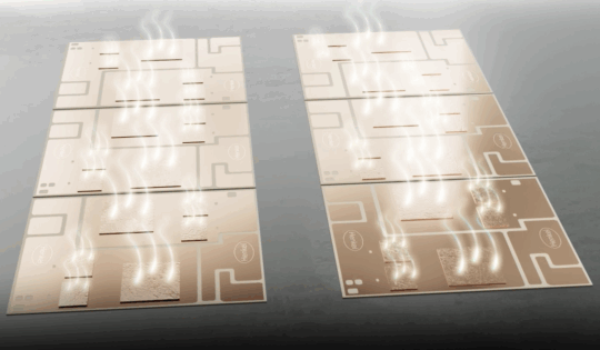
The convergence and synergy of performance and sustainability required to power the next generation of AI data centers The surging...
Henkel Wins Texas Instruments 2024 Supplier Excellence Award
Henkel is proud to announce that it has won the Texas Instruments 2024 Supplier Excellence Award. The most prestigious level...
Henkel and Teca-Print Partner to Drive Novel Pad Printing Solutions in Printed Electronics
Henkel and Teca-Print today have announced a partnership in the pad printing field of printed electronics. The collaboration aims to...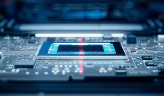
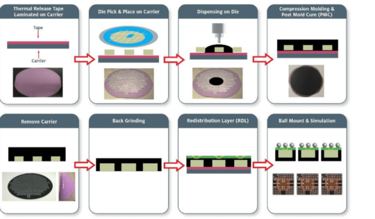
Semiconductor Packaging Materials: The Unseen Marvels of Semiconductors
Semiconductors are the micro-sized “brains” that power modern electronics, and the latest advancements in semiconductor packaging materials are transforming key...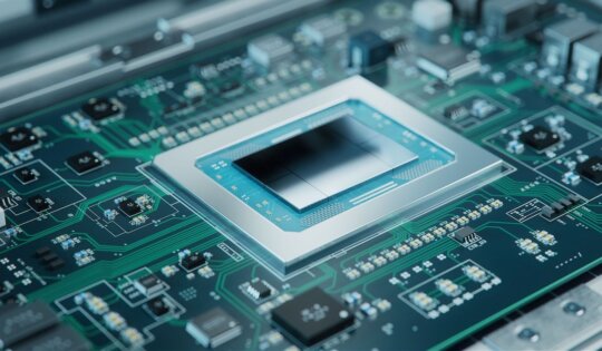
Henkel Semiconductor Capillary Underfill Enables Complex AI and HPC Large Body Advanced Packaging Designs
Irvine, CA – Henkel today announced that it has commercialized a semiconductor capillary underfill encapsulant to address the unique requirements...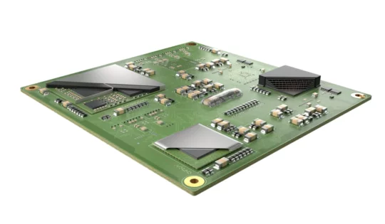
Henkel Highlights Portfolio of Enabling Materials for Next-gen Semiconductor Devices at SEMICON Taiwan 2023
Taipei, Taiwan – At this week’s SEMICON Taiwan, Henkel brings its extensive range of semiconductor packaging material solutions to customers...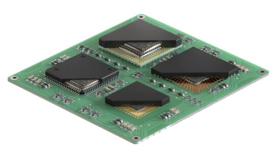
Henkel Debuts Ultra-high Thermal Conductivity Pressure-less Sintering Die Attach Adhesive that Meets Automotive Grade Reliability Standards
Irvine, CA – Henkel today announced the addition of Loctite Ablestik ABP 8068TI to its growing portfolio of high thermal...
Henkel Delivers Versatile, High Thermal Die Attach Adhesive for Power IC Applications
Irvine, CA – As integrated circuits (ICs) become more dense and complex, particularly in the power device sector, new approaches...
3D InCites Awards Program Recognizes Henkel Leadership in Die Attach and Underfill Materials Development
Henkel semiconductor packaging innovations earn Material Supplier of the Year Award Irvine, CA – Henkel today announced that it has...
Henkel Unveils Semiconductor Capillary Underfill for Advanced Silicon Node Flip Chip Applications
Irvine, CA – Henkel today announced the commercialization of its latest semiconductor-grade capillary underfill (CUF) formulation for advanced packaging applications....
Henkel Non-conductive Die Attach Film Offers Broad Wirebond Package Flexibility for High-reliability Applications
Irvine, CA – Henkel today announced the commercialization of a high-performance non-conductive die attach film (ncDAF) engineered to address the...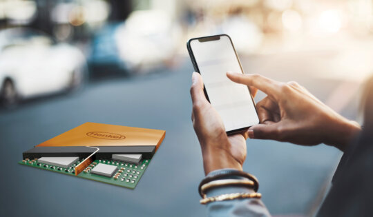
Mobile Antennas and Power Devices that Break the Mold
This paper is co-authored by two of our member companies, Henkel Corporation and LPKF Laser & Electronics AG Laser Direct...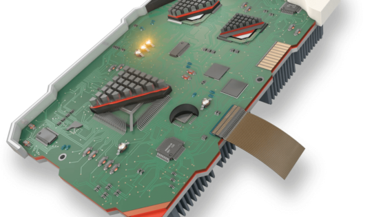
Henkel Unveils Semiconductor Capillary Underfill for Advanced Silicon Node Flip Chip Applications
Highly-filled, fast-flow material balances reliability and processability, extends company’s package-level underfill leadership with multi-format solutions SEOUL, South Korea, Sept. 14,...
Henkel Opens Application Engineering Center for Electronics Applications in South China
Investment to drive localized innovation and to strengthen collaboration with consumer electronics customers. Henkel has officially opened its South China...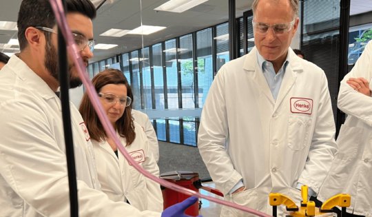
Henkel Opens New Technical Application Center in Silicon Valley to Foster Next-Generation Electronics Development
Irvine, CA – Henkel today announced the opening of its Application Center in Santa Clara, CA designed to support product...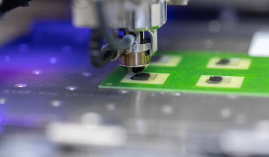
Maximizing Protection of Flip Chip Interconnects with NCP and NCF
NCP and NCF Property Optimization Delivers High-Reliability Results Semiconductor package sizes are getting smaller and bump pitches narrower while the...