
Irvine, CA – Henkel today announced that it has commercialized a semiconductor capillary underfill encapsulant to address the unique requirements of the market’s most demanding advanced packages, like those used in artificial intelligence (AI) and high-performance computing (HPC) applications. Loctite Eccobond UF 9000AE protects large die within flip-chip BGA (FCBGA), high-density fan-out (HD-FO), and 2.5-D advanced packaging devices.
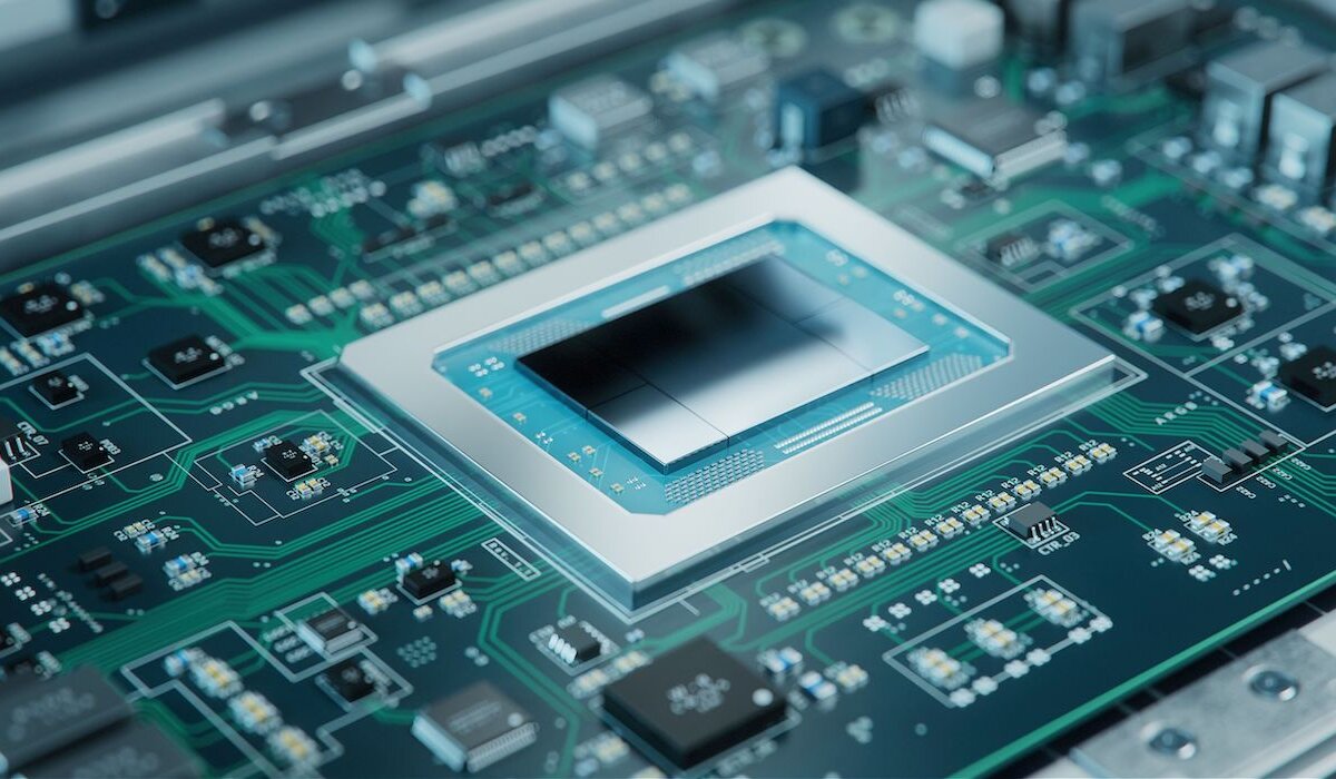
HD-FO and 2.5-D wafer-level packaging techniques have seen significant progress in the last ten years, having achieved dramatic increases in I/O, efficiency, and performance, making them a key enabler of AI growth in the data center and at the edge. With high-density thin, large die (>40 mm x 40 mm) and substantial package body sizes (>100 mm x 100 mm), emerging AI and HPC devices for certain applications can contain more than 2,000 fine-pitch (~100 µm), low gap height (~50 µm) interconnects per die. Bump protection and warpage control are critical for device functionality and optimized package performance. However, achieving thorough bump encapsulation at flow rates that deliver coverage efficiency can be challenging, given the cutting-edge architectural complexity.
Henkel has developed a brand-new capillary underfill formulation that meets the dimensional demands of highly integrated package designs. Loctite Eccobond UF 9000AE completely envelops fine-pitch, low-gap height die interconnects for rigid protection against stress to deliver good electrical, moisture, and thermal reliability performance for high production yields. The material’s low shrinkage and toughness provide die and underfill crack resistance, while its low coefficient of thermal expansion (CTE) protects against warpage. Loctite Eccobond UF 9000AE also has low resin bleed out (RBO) and forms narrow fillets, allowing the dense die integration inherent in advanced packaging techniques.
Henkel Global Market Segment Head for Semiconductor Packaging Materials, Ramachandran (Ram) Trichur, acknowledges that while thorough, rugged bump protection against thermal cycling strain and mechanical damage is the highest underfill priority, processability is critical to achieving throughput and yield objectives.
“Loctite Eccobond UF 9000AE delivers no-voiding bump encapsulation of flip-chip BGA, Cu pillar, and other high-density interconnects, which is fundamental to preserving the value and function of these high-performance devices,” Trichur says. “Notably, however, this material does so faster than our prior generation underfills, allowing for greater flow efficiency, which is an important feature for complete interconnect coverage and encapsulation across large surface areas.”
In internal testing versus previous generation capillary underfills, Loctite Eccobond UF 9000AE demonstrated 20% faster flow* on a 40 mm x 40 mm die, indicating that this material is compatible with even larger die sizes. Its edge-to-edge capillary flow efficiency ensures interconnect encapsulation prior to any material gelation, eliminating the risk of exposed bumps. So far, Loctite Eccobond UF 9000AE’s performance has been validated on die as large as 50 mm x 50 mm and within packages up to 110 mm x 110 mm

“The rise of AI underscores semiconductor packaging ingenuity and its ability to drive remarkable levels of computing power and cost-effective scaling alternatives to Moore’s Law,” Trichur says, citing the well-publicized growth of 2.5-D chip-on-wafer and 3-D advanced packages. “Henkel has been at the forefront of enabling these devices with novel semiconductor materials, and our new underfill further demonstrates our contributions to this dynamic market space.”
Learn more about Henkel’s advanced semiconductor packaging materials at www.henkel-adheisves.com.
LOCTITE® is a registered trademark of Henkel and/or its affiliates in the USA, Germany and elsewhere.


