
In late Feb INEMI hosted a Packaging Tech Topic Webinar: Glass Substrates for Advanced Packaging which was presented by Dr. Dilan Seneviratne and Dr. Gang Duan of Intel Corporation. Dilan Seneviratne is a Principal Engineer and Director of Dielectrics and Surface Prep Area within Intel’s Substrate Packaging Technology Development organization. Gang Duan is a Principal Engineer and Area Manager / Engineering Director for the Backend area in the Substrate Packaging TD organization within Assembly Test TD at Intel. He has been involved with developing EMIB / EMIB-TSV die embedding, as well as HDI substrate backend process, equipment, and materials technologies.
Intel publicly announced its efforts on glass core substrates in Sept of 2023 and we have discussed this in IFTLE 575.
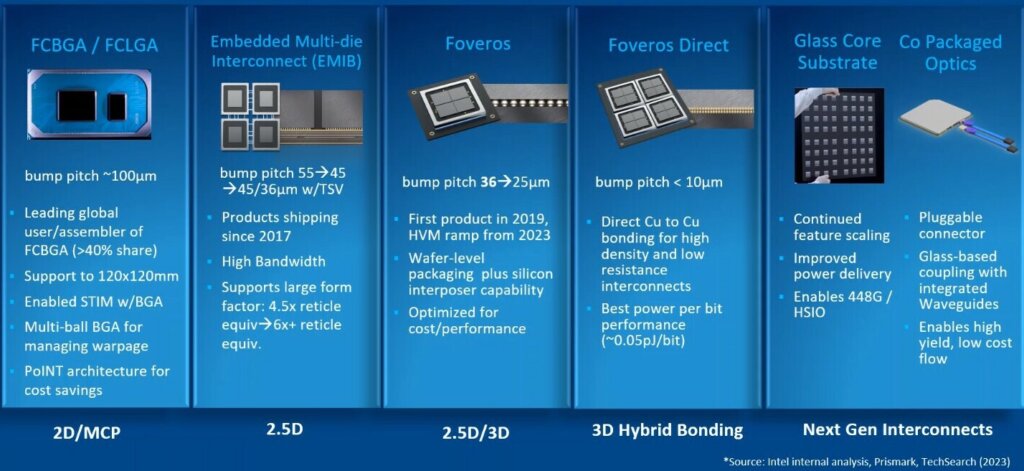
If we look at the latest Intel Advanced Packaging roadmap, we can see that it has added glass core substrates to its roadmap offerings.
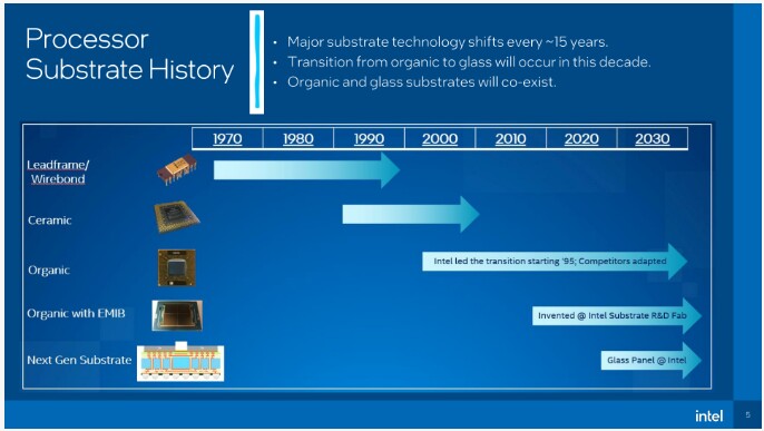
Intel pointed out that there have been major substrate technology changes about every 15 years since the inception of leadframe /wire bond packages in the 1970s as shown in Figure 2.
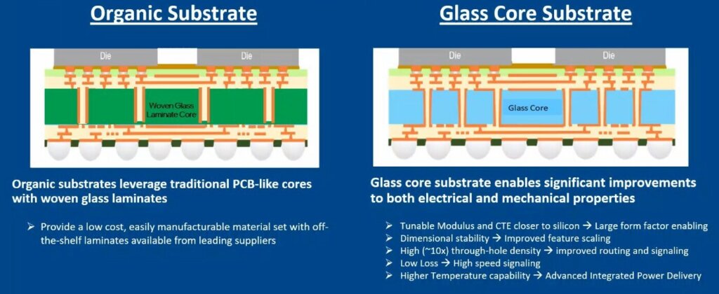
As IFTLE discussed previously (IFTLE 575), Intel’s plan is to replace the traditional woven glass core found in traditional laminates with a solid glass core. The advantages can be seen in Figure 3, such as higher dimensional stability, higher through-hole density, and higher speed signaling.
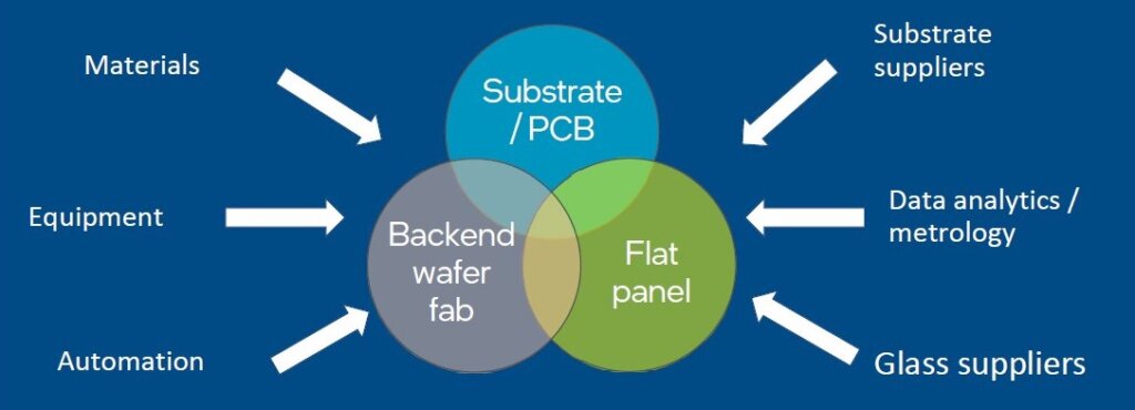
This will require the presence of a “glass package ecosystem” that will include technologies previously developed in the PCB, back-end wafer fab, and flat panel display industries (Figure 4).
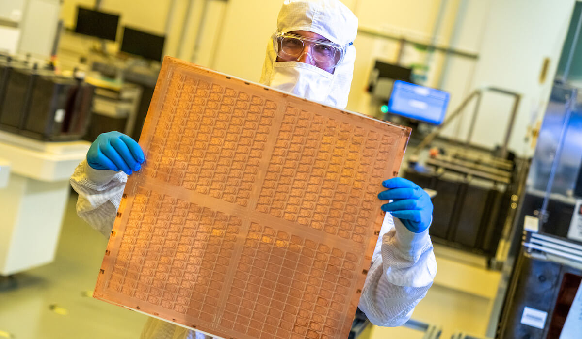
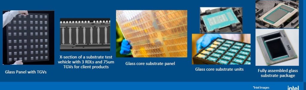
Intel indicates that it has been working on this technology for over a decade and are investing over $1B in a glass R&D line in its Chandler AZ facility. The company says it is working closely with equipment and materials partners to enable the ecosystem. It has developed an electronically functional assembled multi-chip package (MCP) test vehicle with three redistribution layers (RDL) and through glass vias (TGVs) of 75µm. Filled TGVs have a 20:1 aspect ratio for 1mm core thickness, reportedly suited for AI and data center applications. Intel claims to have more than 600 inventions related to architecture, processes, equipment, and materials. (Figure 5).
Several interesting questions came up during the Q&A session:

- One commenter pointed out that TSMC reported at the 2011 IEEE ECTC that “The brittle nature of glass along with its low fracture strength, particularly with TGV, could have serious implications on the reliability of the packaging system using a glass substrate.” Intel indicated awareness of this and is working on the issue.
- Another question inquired as to the dielectric that was being used for the RDL layers. The Intel response was that it is examining a number of possibilities [not just Ajinomoto build-up film (ABF) ] but has not chosen one material yet.
- Intel indicated that this “double-sided process” was “difficult” with glass handling being an issue.
- When asked about reliability data, Intel indicated that stresses are an issue and they are working to minimize them. A company spokesperson stated that they had no reliability data to share at this point.
All in all, IFTLE concludes that anyone anticipating see such structures in Intel commercial production before 2030 should not hold their breath!
But remember, Intel is not the only company looking at such technologies.
Absolics Glass Core Substrates
IFTLE was the first to share with you that SKC (a subsidiary of South Korean Chaebol SK Group) has announced that it is bringing up a $600MM glass substrate production plant in Covington Georgia with plans to expand it to 72,000 sq-meter by 2025 (NOTE IFTLE thinks 2025 for a qualified manufacturing date is also probably a bit aggressive ) (Figure 6)
My main message here is that glass core substrates appear to have made the roadmaps of several major suppliers, significant monies are being spent and they are something should be looking forward to in the future ….
For all the latest in Advanced Packaging stay linked to IFTLE…………………


