
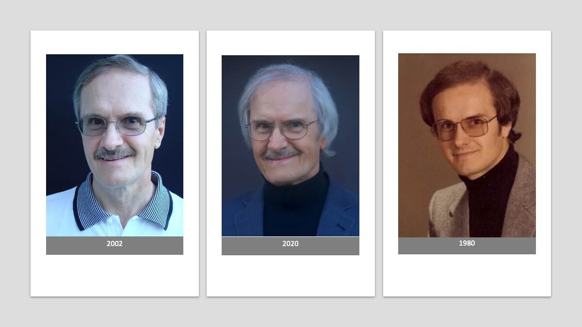
In the Spring 2020 issue of the MEPTEC Report, Herb Reiter briefly emerged from his recent retirement to pen an article and interview based on lessons learned from fifty years in the semiconductor industry. Turns out he had a lot to say. So with Ira Feldman and Bette Cooper’s blessing, we’re publishing it as a series. Six lessons each, and a final Q&A. This second of three parts covers lessons 17-12, plus a big life lesson. If you missed Part 1, find it here.
After three years of alliance management, VLSI’s CTO offered me a strategic product planning position on his team. I became the worldwide missionary for ASIC core technology innovations and market researcher for new ASIC requirements. In parallel with this strategic role, I managed first a development program for a 400+ pin tape-bonded package for the CPU in Apple’s Newton, the grandfather of today’s iPads. When VLSI developed a family of chips for a high-end graphics workstation, they needed 300 to 800 pin high-power packages. I managed the development cooperation between IBM Endicott and VLSI to develop and qualify five tape ball grid arrays (TBGAs) for volume production.
Lesson 7: These two big, important, and highly visible packaging programs showed me how complex and important IC packaging technology is and how critical the right packages are for the success of semiconductors.
The long and expensive development of ASICs encouraged more customers in the 1990s to switch to off-the-shelf application-specific products (ASSPs) for their system designs. VLSI gave me the opportunity to market ASSPs, specifically QAMs, QPSKs, MPEG decoders, modems, and controller chips for digital set-top boxes and other consumer applications.
Lesson 8: Adding intellectual property (IP) to an ASIC increased the IC’s value significantly.
As IC complexities and pin-counts increased steadily and low unit cost became much more important, the need for user-friendly and high-productivity IC design and verification tools increased rapidly. VLSI’s in-house electronic design automation (EDA) team could not keep up with all the new requirements. And VLSI, the former ASIC leader, was no longer competitive and encouraged Philips to acquire them.
Lesson 9: a) It was great to work at an integrated device manufacturer (IDM). I was able to get all needed IC design and manufacturing experts into one room, map out project plans, then manage their execution in regular meetings and with agreed-upon action items.
b) If a company’s capabilities in important areas (e.g., EDA) are not competitive, they need to find competent partners or buy these capabilities externally — otherwise, they will lose market share, get acquired, or die.
As more and more analog circuits got replaced by digital circuits in computers, communication, and consumer products, EDA tools for accurate timing analysis (a.k.a. timing closure) became critically important.
How can a hardware guy in a hardware company (VLSI) address this EDA challenge/opportunity? It was impossible, so I joined ViewLogic, a medium-size EDA company, in Fall 1996. They needed an alliance manager for a small support team (called ASIC Vendor Program) serving the biggest ASIC vendors worldwide in developing libraries as well as evaluating, qualifying, and integrating Motive and two other tools into their design flows. ViewLogic’s best product was Motive, a user-friendly and accurate static timing analysis (STA) solution. Our customers liked Motive and my team’s support. These customers in turn encouraged Synopsys to acquire ViewLogic.
Lesson 10: Walking in the customers’ shoes for almost 20 years – at National and VLSI – significantly helped me to understand their requirements and build strong partnerships between ViewLogic and its key customers – the largest ASIC vendors. All of them were IDMs, like National and VLSI. They had demanding corporate teams for developing libraries and for evaluating, qualifying, and integrating merchant design tools into their product groups’ IC design flows.
At the end of 1997, Synopsys acquired ViewLogic for ~ $ 400 Million. Because the big ASIC vendors suggested it, Synopsys put me in charge of its Semiconductor Vendor Program (SVP) to manage these alliances in the U.S. My now much larger team supported library developments, tool evaluations, and design flow integrations of many tools: PrimeTime, Design Compiler, VCS, Formality, TestMax, and others. We also continued a project I started at ViewLogic jointly with TSMC (a dedicated wafer foundry): we developed TSMC’s first and second reference design flows for fabless IC vendors. In other words, the SVP teams worked with the largest IDMs and fabless/fab-lite IC vendors to develop the infrastructure they needed to quicker and easier design ASICs and ASSPs, using Synopsys tools. Our customers and Synopsys’ top management liked the significant progress my U.S. team made and expanded my responsibilities to include Synopsys’ local SVP teams in Japan, Taiwan, and Europe. However, major differences with my direct boss finally led me to resign. Leaving my great team with 25 excellent engineers was difficult but necessary.
Lesson 11: Your manager’s personal objectives can undermine the success of your company’s most important programs.
In 1999 it became obvious that the emerging internet would significantly impact the semiconductor industry. Early 2000 I joined Barcelona Design, one of the many “.com start-ups”, as alliance manager for its big customers. Our team of highly educated Stanford PhDs really impressed me and our customers. However, meeting the PhDs’ ambitious goal to quickly revolutionize analog circuit design with web-based optimization engines was more difficult than expected. Somebody needed to be blamed for the lack of success. Management chose the only person without a Stanford Ph.D. at Barcelona – and encouraged me to resign. A month later they tried to get me back.
Lesson 12: Analog circuit design is a creative art. Algorithms, computers, and networks could not compete with analog gurus – certainly not at that time and maybe never.
I did not mind leaving Barcelona, because I already had plans to start my own company – to bring developers of EDA tools and big ASIC/ASSP manufacturers closer together…

In early 2002 I founded eda 2 asic Consulting, Inc. to focus on building alliances between small EDA vendors and large ASIC/ASSP vendors. The relationships I had built with these large ASIC vendors at ViewLogic and Synopsys opened many doors for me and my consulting clients. I really enjoyed these rewarding years as a “corporate matchmaker”. However, the 2008 financial crisis encouraged the large semiconductor vendors to focus only on large EDA suppliers. This forced many small companies, including my clients, to cut budgets for consulting services.
While one door closed, another one opened: Many large semiconductor vendors were no longer IDMs but fab-lite or fabless companies [2] and needed to work with partners to build a complete and cost-effective supply chain. They needed industry organizations, like the Fabless Semiconductor Association (FSA), to help to streamline the complex supply chains, accelerating essential innovations, and driving best practices and industry-wide standards.
The FSA, later renamed to Global Semiconductor Alliance (GSA), offered me in early 2008 the opportunity to manage their EDA Working Group. I gladly accepted. After a few working group meetings, we concluded that our focus should be the emerging 3D IC technology. We expected it to require many new EDA tools which would offer EDA vendors new growth opportunities. However, in the following years it became obvious that combining multiple dice in an IC package faces significantly bigger EDA and manufacturing challenges than expected, e.g., heat dissipation, thermal-mechanical forces, power and signal integrity, wafer thinning and bonding/debonding, TSV filling/revealing, die and interposer warping, micro-bump cracking, and many others. All of these increased 3D IC development challenges and unit costs. When the path to profitable 3D IC design and manufacturing flows looked much steeper than expected, the working group lost momentum and stopped meeting at the end of 2012.
Maybe I am crazy, but for me, 3D IC technology is the best opportunity to encourage our component-focused semiconductor industry to design and manufacture much higher value (= more profitable) system building blocks. That is why I consulted with these 3D IC focused industry organizations from 2013 until my retirement in 2020:
- SEMATEC’s 3D IC team to address the development of equipment and manufacturing flows for 3D ICs,
- Silicon Integration Initiative (Si2) to develop 2D & 3D IC design flows, best practices, and standards,
- Electronic System Design (ESD) Alliance to encourage our industry to expand from the component-focused activities and target more profitable system-level building blocks,
- SEMI through my work as a blogger for 3D InCites, a media company. I was able to engage with many of SEMI’s 2000+ worldwide member companies that span all areas of the electronic systems’ supply chain. SEMI teams have initiated and coordinated, so far, more than 1000 manufacturing standards. They are also organizing workshops and conferences on technical and business topics worldwide. And they even play a major role in getting the US government’s attention for our industry’s needs and are working with other countries’ governments. SEMI’s Heterogeneous Integration Roadmap (HIR) efforts are an essential and industry-wide contribution to the proliferation of 3D ICs and advanced packaging technologies.
My almost 20 years of eda2asic Consulting services were challenging but interesting and rewarding. My broad background helped me to learn quickly and contribute in many different ways to each one of the many companies and organizations.
Final career lesson: The most important factor for my success as a consultant was the many friends and supporters that gave me opportunities to be of service. — THANK YOU ALL!
In part three of this series, Herb answers some burning questions about technology breakthroughs, his career, emigrating to the USA, and more. If you can’t wait, you can find the full article in its entirety in the MEPTEC Report.


