

During in-person and on-line meetings, I often discuss with friends the impressive progress our industry has made in the last 50 years following Moore’s Law. In 1981, when I joined the industry, on-die feature sizes were 3 microns (= 3000 nm). Today, some IC designers already rely on 3 nm features to integrate billions of transistors on a single die. However, until a few years ago, we rarely talked about the enormous progress the IC packaging industry has made in regard to pin/ball count and pitches, max power dissipated in a package, reduction in package footprint and height, power and signal integrity, cost per pin, etc.
Today’s market needs for much higher integration than a single-die SoC can offer economically, have finally drawn a lot of attention to the significant progress the IC packaging industry has made and clearly demonstrate how a big part of the total IC value creation is moving from the die/dice to the package.
How IC Packaging Technologies have Evolved
At the recent MEPTEC/iMAPS webinar, Brandon Prior, Senior Consultant at Prismark Partners LLC, gave an excellent overview of how IC packaging technologies have evolved and are contributing to our industry’s progress. He also showed how advanced packaging technologies are pushing printed circuit board (PCB) suppliers towards smaller pitches, better power integrity, and thermal conductivity, to name a few. Shrinking package and board geometries significantly reduces parasitic capacitance and power dissipated in interconnects, resulting in much higher performance per Watt, longer battery life for handheld devices, and lower system cost.
Key Market Trends
Computers are a big, but no longer the most important market for semiconductors. Many other electronic systems rely on ICs to increase the number and quality of features, improve safety, reliability, and enable user-friendly operation. In Figure 1, Prior showed the diversity of applications, specified current revenues, and growth potentials.
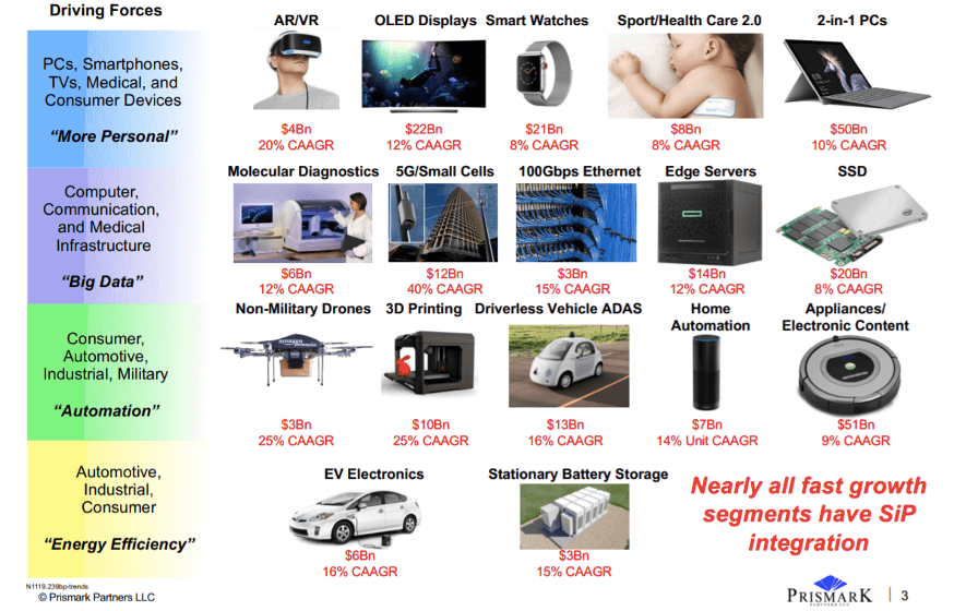
Prior also discussed how the major markets – data centers, automotive, consumer, industrial, medical, wearables as well as PCs – will grow and consume ICs. How will different package types grow? He predicted that by 2030 70% of the IC packages will still use wire bonding because many fully depreciated wire-bonders keep the assembly cost for small to medium pin-count packages low. For higher pin-counts flip-chip technology is dominant. In the last few years, wafer-level packaging has become a cost-effective and space-saving alternative. Panel-level packaging is in development, to further reduce unit cost. Prior showed how the different package types are constructed, explained their benefits, and suitability for specific applications.
Smartphones and Wearables Drive IC Packaging and PCB Geometry Reductions
To demonstrate how the ~ 1 Billion/year smartphones drive IC packaging and PCB technology, Prior showed several mother and daughter board teardowns, with components mounted on both sides. The pictures also showed that besides ICs, passive components, camera modules, connectors, and of course the large battery compete for space in a phone. To reduce IC body sizes, ball pitches have gone from more than 1 mm to 0.4/0.35/0.30 mm, depending on the application. He stated that most major IC vendors can now offer 0.25 mm ball pitches, for mounting on high-density PCBs. When Prior showed teardowns of Apple iPods and watches, he emphasized that these use pitches down to 0.22 mm but require expensive assembly equipment to achieve high yields and reliability. Prior stated that many PCBs in use today still have 65-75 um line/space pitches, sufficient and cost-effective for a broad range of applications. Substrate-like PCBs (SLPs) allow 25-30 um L/S but require more costly equipment. Miniature passives (e.g. with 0.1/0.05 mm length/width) for mounting on interposers, substrates, and SLPs also contribute to electronic devices with smaller form factors.
To define the difference between a module and a system in package (SiP) Prior suggested:
- A module contains one or more bare dice and other components, to form a functional electronic block
- A system-in-package (SiP) comprises multiple modules
Prior also showed and discussed an informative table with Memory SiPs, RF Modules, PMMs, and many other functions, their primary applications, and projections for 2019 –’24 growth rates.
Considering that each 5G mm-wave (FR2) phone needs multiple RF modules that contain a power amplifier (PA), passives, filters, switches, and the antenna. Prior expects that market demand for these modules will rapidly increase. He also pointed out that FR2 phones and lidar systems operate at frequencies up to 70 GHz and require compartmental or global shielding of components to avoid/minimize interference and pointed out that the demand to integrate photonic functions in a package is rapidly increasing too.

His summary showed that not only smartphones and wearables drive packaging technology, but also high- performance computing and high-speed communication markets. Data centers require integration of heterogeneous functions (logic + memory + transceivers + optical components) in high-power (10s of Watts) packages.
Personal Comments
When I started in 2008 to focus on 3D-ICs and IC packaging in general, I was impressed but also concerned about the many package types in use. Packaging experts explained to me that most IC designs at that time were started without the package in mind. A completed die design was “thrown over the wall” to a packaging company that had to custom-design a package and make sure that the die – package “combo” met market requirements. This time-consuming and costly adaptation process demanded many iterations, wasted development time and money, and often caused tensions, even serious conflicts, between the die and package design teams.
I am glad to see that major IC packaging houses and foundries are now working with EDA partners and major customers, to jointly develop package assembly design kits (PADKs) and die-package-board reference design flows. While PADKs specify important materials/equipment/assembly-process and test capabilities and list off-the-shelf packages, reference design flows enable die, package and board designers to exchange design data upstream and downstream and simulate how to develop the most cost-effective, highest-performance, lowest power, smallest, most reliable,… die-package-board solution.
Only such a well-coordinated supply chain will be able to meet the technical challenges of complex multi-die IC designs and bring attractively priced ICs and sub-systems to market, timely, and cost-effectively.
Prior’s presentation gave an in-depth look at the significant progress IC packaging experts have made in recent decades. It also left no doubt, that the pace of IC packaging innovation can only accelerate and demand more planning and coordination, between customers, EDA/equipment/materials suppliers, and industry organizations, like SEMI. ~ Herb


