
Each year as SEMICON West approaches, I look forward to the IMEC ITF USA event. For the past several years IMEC has been one of the kickoff events for SEMICON West. This year was no different, IMEC just kicked things off a bit early, holding the ITF USA 2020 virtual event on July 7 instead of SEMICON week.
One of the things I enjoy about the IMEC event is that you get a good overview of the technology roadmap and what some of the brick walls, to use an old Sematech term, are and what programs IMEC has in place to address those challenges.
For those reading this post who are not familiar with IMEC, they are one of the leading semiconductor research consortiums and are based in Belgium. IMEC typically selects a project that is pertinent to the Industry and opens an invitation for companies to join them in the research effort. These projects have been essential in helping the semiconductor industry continue to shrink along the lines of Moore’s Law, but also have created significant “More than Moore” research projects to help the industry resolve some of the critical issues facing power and communication semiconductors.
This year’s ITF USA did not disappoint, due to the virtual nature of the event IMEC was able to include some of the projects they are working on in mini-interviews/presentations that gave the audience a good idea of what work was taking place, and giving companies the opportunity to partner with these researchers. The researchers presented in a concise manner, similar to what you would do at a trade show in the booth, you then had the opportunity to chat with the speaker to ask deeper questions. Topics covered were AI Chip, Quantum computing, IMEC. IC-link ASIC services, Optical Beamforming, Silicon Photonics, and System-level reliability for SOC.
Yes, The Industry is Still Working on Shrinks
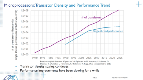
IMEC has had a research focus on integrated circuits, as well as on healthcare for as long as I have been associated with them, this ITF USA was no different. Luc Van Den Hove the president and CEO of IMEC kicked things off with an overview of where the industry is headed from what is driving IC technology and what IMEC is doing to help the industry develop technology for those drivers. It all begins with the transistor and the industry being able to continue making transistors smaller faster and cheaper. In recent years the industry has needed to address the power, performance, area, and cost (PPAC) challenges. Since 28nm the cost to make transistors has been increasing, but the industry has managed to mitigate the cost and performance declines with new technology such as finFETs and materials to keep the performance and cost close to the original curves; however, even with the PPAC to accomplish drivers such as analytics, AI, augmented reality, 6G, and a more seamless user device experience, smaller transistors are still needed.
So, for those that are banging the gong that “Moore’s Law is Dead”, there is still life, from a shrinking perspective, even if the PPAC does not follow the traditional curve. Sub 1nm which is a 7x shrink from today’s leading-edge production, could emerge in some pilot lines in less than 0 years.
Van Den Hove laid out the transistor road map to below 1nm, and the proposed lithography road map to get there. The transistor road map moves from finFET to nanosheets, to Forksheet to CFET, to 2D materials in the Channel. The roadmap moves the industry from the current 7nm technology node down to below 1nm at a rapid pace.
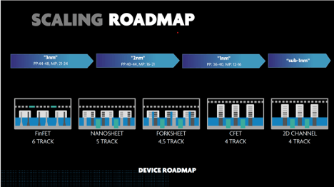
To reach below 1nm transistor new architecture, 2D Channel, materials, WS2 and lithography, high NA EUV, techniques will need to be developed to achieve sub 1nm technology. Van Den Hove touched on this topic and then Martin Van Den Brink of ASML presented on the progress taking place in EUV lithography.
Packaging is Critical to Achieve AI and Data Center Goals
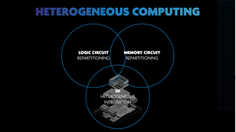
However, to successfully meet the performance needs of AI, neuromorphic computing, and to reduce the energy consumption required for AI learning systems, significant changes to the layout of logic and memory are needed. Today’s systems on chip (SoC) have a memory bottleneck. This can be resolved by the 3D integration of logic and memory into the same package, but getting the memory closer to the logic is critical to help to improve system performance. Heterogeneous compute or 3D heterogeneous integration where the logic and memory are bonded directly to each other to create, or at least placed in close proximity will produce a system with increased performance and lower power. Both are critical for improving the AI learning process and reducing the amount of power needed for both the learning step, but also the inference portion of AI.

Sick Care to Health Care
As mentioned earlier Healthcare has a strong focus at IMEC. Van Den Hove presented on several applications IMEC is working on. Using the smart pill, which has been around for a bit, IMEC developed the first millimeter-wireless transceivers for the immediate communication needed for smart pills. IMEC is developing wireless power transfer for ingestible and implants. This can potentially eliminate the need to replace a medical implant by surgery which always carries some risk.
Lab work is always a slow part of the medical process, IMEC presented a nanofluidic processor that can be analyzed with an onsite point of care diagnostic tool that is projected to take the analysis time down to a few minutes from the hour that benchtop analysis typically takes. The initial technology may be more expensive than the average person can afford, but think of having your blood work performed in the Dr. office, and getting your results nearly immediately, as opposed to waiting hours or days before the analysis is complete. Van Den Hove pointed out that if we could have nearly immediate feedback for something like Covid-19 or the next potential pandemic,
Using the example of the virtual meeting, which by no means replaces attending a conference in person, Van Den Hove looked to the future for what might be the ultimate virtual experience, and what the industry currently understands those tools to be. VR/AR for visual and sound, mid-air haptic feedback for touch, and the potential for hologram use to have a 3D visual experience. All we need now is smell and taste, and it will almost be like being there.
And There was More!
While I have only focused on the keynote here, the follow-on presentations supported Van Den Hove’s position, and then also devolved deeper into the subjects Van Den Hove touched on.
- Next-generation communications for 6G, which are needed for the tremendous transfer of data that is emerging at 5G and will continue forward.
- Scaling and the lithographic tools needed to scale, which have been discussed above for integrated circuits. But also scaling for packaging and interconnect to better facilitate 3D integration and to continue to make the form factor smaller
- Post Moore Semiconductors, which touched on future 3D nano-system integration, and other future research.
- And Photonics, which if can finally be realized will be a major contributor to reducing the energy in data centers and enable data to be transferred at much higher speeds than today.
The title of Van Den Hove’s talk was “Leap into the Semiconductor future”. As the 2020 unofficial kick-off to Semicon west Van Den Hove and the IMEC organization has done an excellent job of setting the stage for the next 10 years of semiconductor development, as the industry leaps into SEMICON week.


