
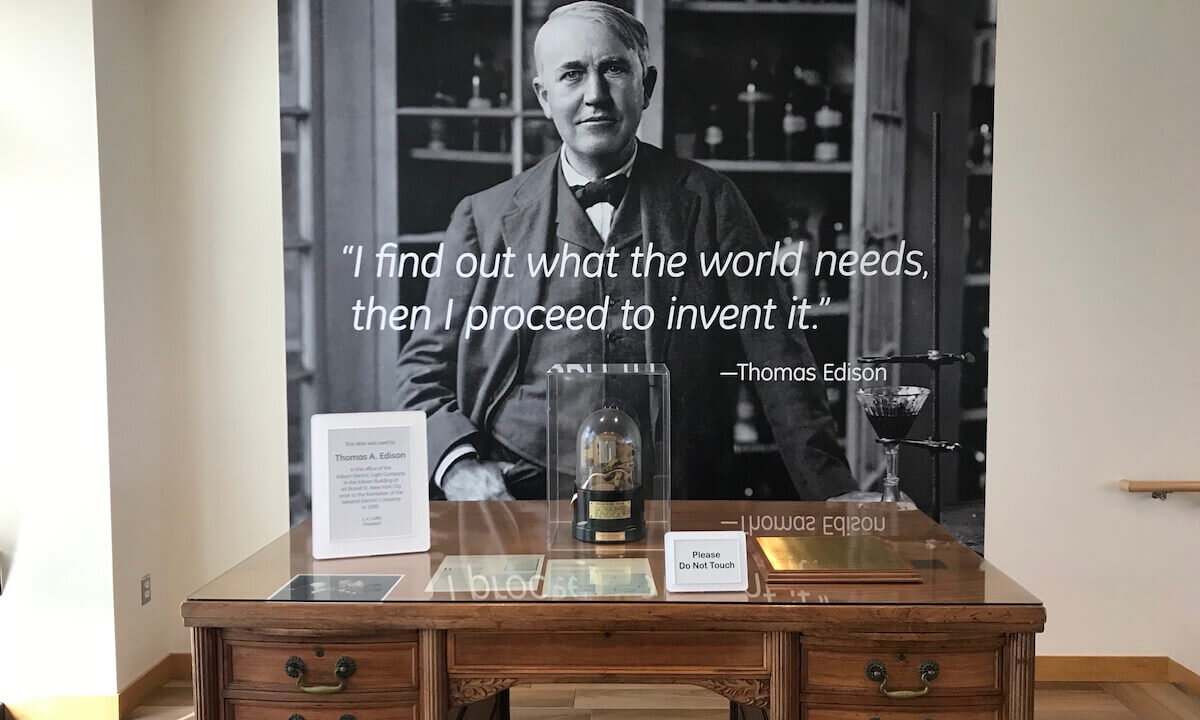
Thomas Alva Edison didn’t invent semiconductor device packaging, but he might have, had he lived just one more generation.
“I find out what the world needs. Then I go ahead and try to invent it.”*
Edison passed away in 1931, less than twenty years before John Bardeen, Walter Brattain, and William Shockley invented the transistor at Bell Labs in 1947, starting our electronic age.
Bring to your mind again images from those photos you’ve seen of the very first transistor: the device is just hanging out there in free space, naked, rather primitive looking, an arrowhead pointing down, trailed by a squiggle of wires, an arrow’s crazy fletching.![]()
This first transistor functioned, and its inventors received the 1956 Nobel Prize in Physics for their work, but, in order to be of practical use, that first transistor needed to be packaged.
“Anything that won’t sell, I don’t want to invent. Its sale is proof of utility, and utility is success.”
I like to imagine a historic rivalry between Bell Labs and GE Research, Alexander Graham Bell and his team facing off against Edison, aka the Wizard of Menlo Park, and his squad, sleeves rolled up in New Jersey and New York State, going round after round, diving deep into basic science and then inventing the technologies that inform our world today.
In Edison’s case, it was a matter of inventing or discovering the why of science itself, and it was also the discipline of his in applying consistency to the way of inventing that lives on, creating the model we follow still today just about everywhere for the how industrial R&D should be done.
“Being busy does not always mean real work. The object of all work is production or accomplishment and to either of these ends there must be forethought, system, planning, intelligence, and honest purpose, as well as perspiration.”
We stand on the shoulders of giants.
“A genius is often merely a talented person who has done all of his or her homework.”
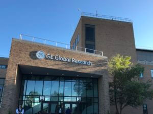 GE Research in Niskayuna, NY, was the venue for the 31st. Annual Electronic Packaging Symposium, co-organized by GE and by Binghamton University’s Integrated Electronics Engineering Center, under the aegis of the IEEE Electronics Packaging Society. EPS attendees met on September 5 and 6, 2019 for two days of talks, two days of a parallel vendor exhibition, and, for those who stayed on, an afternoon program devoted to a Heterogeneous Integration Roadmap Workshop, including updates on the MEMS TWG (HIR lingo for Technical Working Group), the Single & Multichip Integration TWG, and the Mobile TWG.
“When I have finally decided that a result is worth getting, I go ahead on it and make trial after trial until it comes.”
We were encouraged to not take photos during the keynote and other presentations, and the EPS 2019 Proceedings won’t be out for another couple of weeks, but while the talks are still fresh in my mind, let me please offer you highlights from my notes, in the form of these bits of overheard wisdom.
Let’s start with this lighthearted remark by James LeBlanc, Global Technology Leader, Electronics, GE Research, in his opening remarks: “Whenever something’s not working in the electronics world it’s the packaging guy’s fault.” (This makes me wonder whether the early Bell Labs transistor continued to work once it was packaged. If not, it was surely the packaging that was at fault, right? No Nobel there …)

The EPS 2019 opening keynote talk by Mukesh Khare, Vice President, IBM Research, deserves a blog all its own; speaking on “Technology Innovation for the AI Era,” Dr. Khare voiced what will perhaps become 3D InCites’ new rally cry: “The world has become heterogeneous.”
Can you name three beautiful ideas of active interest in electronics today? Me, I like the three identified by Mukesh:
- Bits, and the work we have done to date and continue to do ensuring continued progress in digital circuits
- Neurons, work that is the basis of AI and Machine Learning, still in its infancy for the most part, but moving soon from Narrow AI to Broad AI to General AI, which will become ubiquitous in 2050 and beyond
- Qbits, those strange things (strange to me at least), but strange not for long, for “If nature is Quantum, not Classical, then the only way to solve problems is with quantum computing.” And it is quantum science that we must pursue to do it.
(More about that from the American Vacuum Society: “There is growing excitement around quantum information science (QIS): the White House Office of Science and Technology Policy released a preliminary national QIS strategy in September and the U.S. Department of Energy and the National Science Foundation awarded $249 million in QIS grants; funders around the globe are allocating almost $15bn to QIS over the next few years.”)
Ready for “The Age of Automobility?” It’s coming, Transportation as a Service (TaaS?) is, according to Joseph Kolly, Chief Safety Scientist at the National Highway Traffic Safety Administration. The value proposition for implementing Advanced Driver Assistance Systems (ADAS) is compelling: ADAS has the potential to eliminate the one hundred lives lost per day, on average, just in the United States alone as a result of automobile accidents, much less the many more daily traffic deaths incurred across the world. (According to the WHO, “Over 3,700 people die on the world’s roads every day and tens of millions of people are injured or disabled every year.”)
But people are afraid of robots … go figure.
It was standing room only for the talks John Hunt, ASE, and Rahul Manepalli, Intel, gave on their respective progress with fan out packaging, whether it be classical wafer-level or the soon-to-be-rolled-out 600mm x 600mm panel-level fan out (ASE), or the multiple generations of Embedded Multi-die Interconnect Bridge (EMIB) packaging Intel has released. Per Rahul, “EMIB looks easy in a cartoon, but it’s not that easy to make it.” Kudos to Intel for the many years of debugging that has yielded EMIB volume production. Edison would be proud.
And how is it I can imagine Thomas Edison as the father of advanced packaging? Think of what many say is Edison’s greatest invention: commercial incandescent lighting.
The Department of Energy offers us this capsule history of the commercial light bulb: “More than 150 years ago, inventors began working on a bright idea that would have a dramatic impact on how we use energy in our homes and offices. This invention changed the way we design buildings, increased the length of the average workday and jumpstarted new businesses. It also led to new energy breakthroughs — from power plants and electric transmission lines to home appliances and electric motors.”
 After something like forty years of tinkering, which resulted only in still expensive light bulbs of very limited service life as a result of premature filament failure, “… Edison and his researchers at Menlo Park … focused on improving the filament — first testing carbon, then platinum, before finally returning to a carbon filament. By October 1879, Edison’s team had produced a light bulb with a carbonized filament of uncoated cotton thread that could last for 14.5 hours. They continued to experiment with the filament until settling on one made from bamboo that gave Edison’s lamps a lifetime of up to 1,200 hours — this filament became the standard for the Edison bulb for the next 10 years. Edison also made other improvements to the light bulb, including creating a better vacuum pump to fully remove the air from the bulb and developing the Edison screw (what is now the standard socket fittings for light bulbs).”
In a sense, Edison perfected both a commercial device, the incandescent filament, and its package. And we honor his achievements. From Pittsburgh, PA, thanks for reading. ~PFW
*All TAE quotes courtesy of the Edison Innovation Foundation.


