

California’s Wine Country attracts visitors from all over the world. They can enjoy the scenic countryside, historic places, golf courses, tennis courts, gambling and of course great wine and excellent food. How well can a highly technical conference compete with all these “distractions”? Please read about the sessions I attended and judge for yourself!
The Inaugural Conference and Exhibition on System in Package (SiP) Technology was organized by IMAPS and chaired by Amkor’s Nozad Karim. Very competent presenters conveyed information about how well development efforts worldwide are proceeding to prepare the semiconductor industry for the “More-than-Moore” era of heterogeneous integration.
As “inaugural” indicates, this kind of very focused SiP conference has never been tried before. In his opening speech on Tuesday morning, Karim highlighted the past, present, and future of SiP technology and set the stage for three days of very technical presentations.
How to best convey the importance of a new technology? With market data! That’s why Jan Vardaman from TechSearch International took the stage next and substantiated the market needs and reasons for SiP adoption.
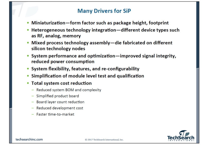
In addition to discussing the SiP drivers listed here, Vardaman projected a 13.7% CAGR for SiP technology from 2016 to 2020. Especially wearable electronics for consumer and medical applications will benefit from SiP capabilities. She sees design tools, material capabilities and manufacturing flows as the major factors constraining SiP revenue growth.
David Lu, an executive from Huawei, talk about their capabilities and challenges as SiPs suppliers for mobile devices, primarily smart watches. It was fascinating to see how many functions these devices can pack into a very small space and how many companies now have smart watches in volume production that far exceed Dick Tracy’s marvel. One very important point became clear to me during Lu’s presentation: These watches need antennas – and yes, antennas can also be integrated into these tiny SiPs.
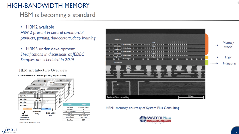
YOLE’s founder, Jean-Christophe Eloy, showed us the growing number of companies now complementing his market research team. Among them is SYSTEMPlus Consulting, focused on teardowns. Eloy showed their analysis of high-bandwidth memory (HBM (Figure 2). Just like I experienced in the mid-1980’s in the ASIC business, memory is again the most important function to complement logic in SiPs. I dare to predict that, like during the ASIC wave, other IP building blocks will follow soon. Unlike in ASIC, they won’t need to be implemented (and constrained) using the SoCs’ logic process. Die-level IP building blocks will be manufactured in the most appropriate process to minimize cost while maximizing performance per Watt.
Yang Zhang, Senior Engineering Director at Qualcomm, gave us a power user’s perspective of SiP technology. He warned about the increasing complexity of the supply chain and suggested that only improved communication and cooperation across company boundaries will enable us to pack hundreds of components into a SiP and manufacture it cost-effectively.
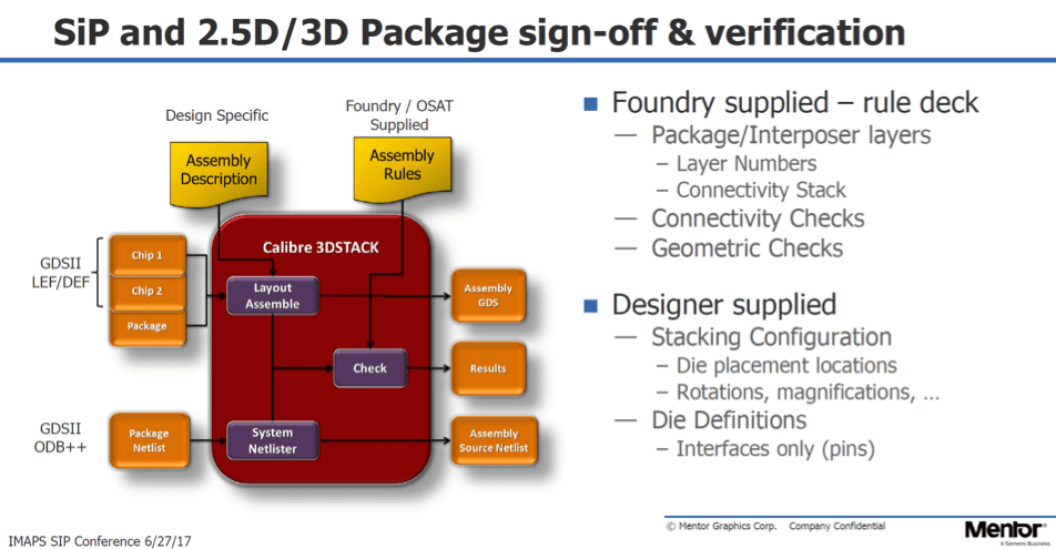
Kevin Rinebold represented Mentor, a SIEMENS Business. He listed many high-density advanced packaging (HDAP) design challenges and explained Mentor’s way of solving them. Like the many 2D SoC focused members of the Calibre family of products, Calibre 3DSTACK, offers a reliable way to verify SiP designs before handing them over to manufacturing.
Figure 3 below, courtesy of Mentor, shows that the intended as well as unintended parasitic interactions between all SiP components need to be checked, before prototyping and later volume production can start.
As frequencies, pin-counts, and the power dissipated in SiPs are rapidly increasing, new packaging materials are needed to take full advantage of the many SiP features and benefits. The Tuesday afternoon keynote, presented by James Fahey, the president of Dow Chemical’s Material Group, conveyed how well Dow, a $ 50 Billion corporation, is aware of our industry’s requirements for new and better materials. Special thanks to Rozalia Beica at DOW for her efforts to raise awareness and understanding of our needs at this large corporation.
Christopher Barrett, CTO of Insight SiP, demonstrated that his company is totally focused on solving SiP-related challenges. He briefly introduced his company, showed the breadth of SiP designs they have contributed to and walked us through the industry’s evolution from multi-chip modules to today’s smart watches.
Hannes Voraberger, director R&D at AT&S in Austria, titled his Wednesday morning keynote “All-in-One Package” and demonstrated how far his company has already progressed toward this goal. Figure 4 below, courtesy of AT&S, shows two strategic directions guiding them to reach this target.
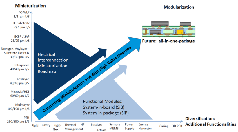
AT&S focuses their core competence — embedding active and passive components within a PCB — in two markets: Mobile devices, like watches, smartphones, and tablets, as well as industrial, automotive and medical applications. Voraberger showed a long list of market leaders they serve and explained clearly why they are growing so quickly.
Karim Arabi from Atlazo Inc. outlined his company’s focus on developing ultra-low power platforms and solutions for medical and consumer IoT applications. He explained why modular SiP solutions, comprised of heterogeneous functions, will be a better fit for many IoT edge nodes than typical SoCs.
Javi De La Cruz, engineering VP at Invensas, a division of the newly formed Xperi corporation, focused his talk on how to meet 5G requirements with their bond via array (BVA®) technology. It allows much tighter component integration than traditional wire bonding, reducing form factor and power dissipation, especially at higher frequencies.
John Bongaarts from National Instruments presented examples why and how SiP solutions disrupt traditional test flows, due to heterogeneous functionality, high complexity, and advanced packaging technologies. He showed how NI’s test equipment and the supporting software enables exhaustive, even system-level test (SLT) of SiPs.

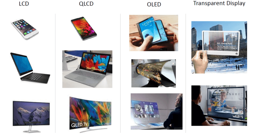
Stefan Peana from DELL gave us a system designer’s perspective of the user benefits SiPs offer for displays. As Figure 5, courtesy of DELL, shows, there are many different applications for displays and quite diverging requirements. The modularity of SiPs gives display designers the flexibility to quickly adapt display drivers to a specific application.
The afternoon sessions started with a presentation from Steffen Kroehnert, Nanium. He started with a slide confirming that on May 22 the Nanium acquisition by Amkor has been concluded. He used the slide in Figure 6 below, courtesy of Amlor/Nanium, to show us the diversity – and flexibility – of packaging solutions.
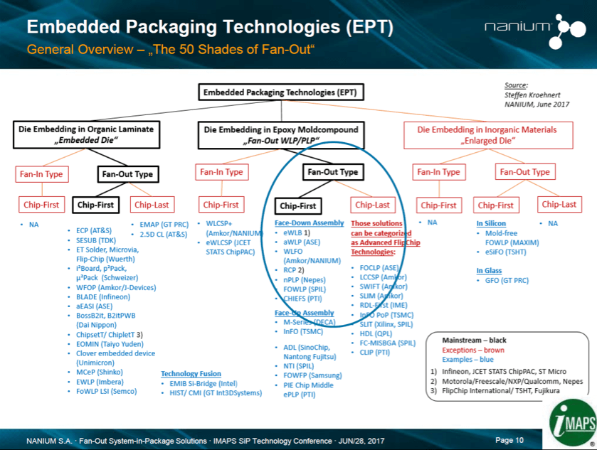
After this “diversity shock-treatment,” he calmed us down by mentioning that packaging standards are in progress and are likely to somewhat narrow down this broad range of choices. In addition, the availability of platforms will reduce NREs and time to market for customers’ designs and encourage the use of “off the shelf” solutions.
Steven Kummerl from Texas Instruments showed the progression of packaging technology in the last ~50 years and explained how TI is using SiP technology to combine analog and digital function with passives in a package, as their customers demand ever smaller, faster and of course lower cost solutions.
Wednesday evening most attendees jumped on a bus to leave for a Wine Country Tour and dinner. I had to miss it and can’t give a first-hand account of it. I only heard that everybody had a really good time.
Thursday morning started with an integrated passives presentation from STATSChipPac’s Jacinta Aman Lim. She explained key advantages IPDs offer (smaller form factor, higher Q inductors, lower power dissipation,…) and outlined STATSChipPAC’s broad range of IPD solutions and development services.
Zuken’s Narajan TV talked about their range of PCB and package design tools and gave several examples how their CR8000 SiP design solution contributed to reducing design time as well as development and unit cost.
Patrick Desjardins from KLA Tencor complemented all other presentations with a metrology perspective. Tighter geometries and smaller tolerances make accurate measurements more difficult, time-consuming and increase unit cost. He outlined the development efforts at KLA Tencor, to meet customer demands and showed a few examples for successful failure analysis with their metrology equipment.
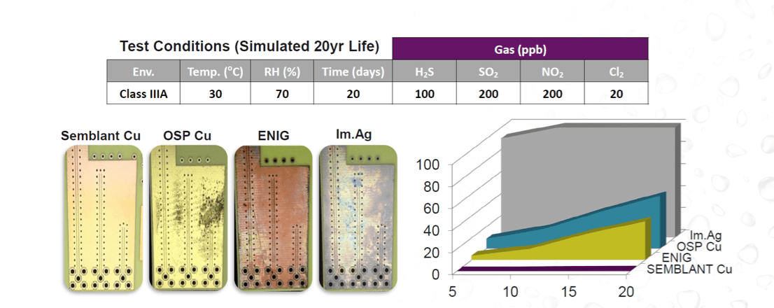
Simon McElrea, CEO of Semblant, surprised many of us when he described how effective their nanomaterial is in protecting electronic devices, modules, and components from moisture and other environmental hazards. Figure 7 below, courtesy of Semblant, compares test results using different protective coating materials.
Henkel’s Jason Cheung addressed another topic that’s gaining importance as components are packed very tight: EMI shielding. He outlined the coating/shielding materials Henkel offers and explained their benefits.
Brian Schmaltz from Namics covered another very important topic for SiPs: Underfill materials. He outlined the thermal, electrical and thermal-mechanical characteristics of these very important substances.
After Thursday’s lunch, a very interesting panel discussion started. Patrick Desjardins from KLA, Derek Floyd / Advantest, David Jandzinski / Qorvo, Gerard John / Amkor and John Park / Cadence gave brief positioning statements, then answered questions from the very knowledgeable audience. I paid so much attention to the topics discussed, that I didn’t have time to take notes, so I can’t report discussion details here. Allow me to summarize the panel discussion and the conference overall with a look back at my ten years of promoting the integration of heterogeneous functions into an IC package:
- We started with learning why our industry would ever need “More than Moore”
- Then we got wrapped up in all the new requirements of this massive shift of paradigm and paused
- As most of the suppliers operate independently, lots of time and energy were spent to catch up or wait for other to complement developed capabilities and make them part of a good SiP solution
- Several leading-edge customers (e.g. AMD, Nvidia, Qualcomm, …) started to focus suppliers on their core competences and coordinated their complementary strengths to get to real solutions
- Suppliers improved their technically compelling solutions and demonstrated lots of reliability data
- As we recognized that lower unit cost was also needed to enable broad market acceptance, massive cost reduction efforts started and suppliers started to work closely together to find where and how to best cut cost
- As development cost and yield challenges of ICs with single digit feature sizes reduced the number of potential users significantly, more and more companies decided to join the “More than Moore” club. This broad market acceptance will bring economies of scale to these solutions, further reduce cost and expand the user base.
This panel discussion demonstrated that all panelist and most of the audience have reached phase 6 or 7.
I look forward to next year’s SiP conference to see how much more progress the SiP supply chain has made and hope that we’ll also attract more customers to report their successes with SiP solutions. ~ Herb


