
Sitaram Arkalgud, VP 3D technologies, Invensas, provided the entertainment at last week’s IWLPC 2015. As soon as he realized Phil Garrou wasn’t in attendance, he reverted to using the 2.5D terminology, despite the fact that on numerous occasions, I have voiced my disdain for the term, preferring “interposer integration.” Arkulgud responded to my catcalls from the audience with, “I’m more afraid of Phil than you!” Fine. Just fine.
For his keynote presentation, Arkalgud was charged with defining the various interposer and 3D stacking variations, and examining low-cost alternatives. He began by comparing various elements of the two approaches, demonstrating that that there are more similarities than differences between the two. Both require bonding and thinning processes, and both can accommodate homogenous and heterogeneous integration. 3D stacking doesn’t require an interposer, but interposer integration offers a bit more versatility than 3D stacking, because it can be accomplished with or without TSVs, and can accommodate both side-by-side configurations and vertical stacking (the AMD Radeon Fury is the perfect example of this).
Despite the fact that interposer integration and 3D stacking are gaining traction in a number of semiconductor applications, Arkalgud says cost is the foremost concern with penetration of these technologies for mobile and consumer applications. The question is, with all the advancements in fan-out wafer level packaging (FOWLP) offering high performance alternatives, why do we still care about interposer integration and stacking in consumer applications? Because whether we want to acknowledge it or not, 3D is now a part of life, and there are some cases where there’s no other way to meet high performance and low power requirements.
For those who argue 3D TSVs have not hit high volumes, take a look at how many 3D image sensors and MEMS devices are in our smartphones, providing higher quality images than ever before, and helping us to navigate to our destinations via Google maps, and making social media applications easier to use. These may not be high density applications, but they are 3D, nonetheless.
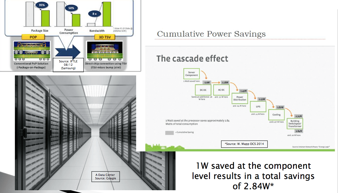
In high performance computing applications, 3D TSVs are found in FPGAs; GPUs; various flavors of DRAM including DDR4, high bandwidth memory (HBM), and the hybrid memory cube (HMC); CPUs (Intel’s Knight’s Landing) and NAND (Toshiba’s nine die stack – eight layers with TSVs). Arkalgud explained the cascading effect millions of CPUs with improved performance at lower power has. He called it “cumulative power savings” (Figure 1). Essentially, 3D already affects everything we do today, says Arkalgud.
Still, if interposer integration and 3D stacks ever want to make it consumer applications, cost must come down. Both interposer integration and stacked DRAM suffers from a slow, expensive assembly process with high CapEx. Additionally, there are still thermal considerations and reliability concerns, as well as micro-bump scaling limitations.
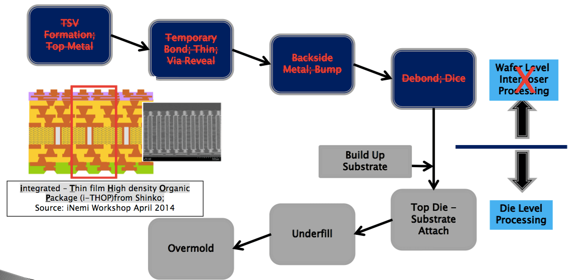
Arkalgud walked us through chip-to-wafer, and chip-to-chip, process flows for interposer integration, identified pain points, and also looked at low cost alternatives being developed. Both SPIL’s silicon-less interposer technology (SLIT) and Amkor’s (SLIM) eliminate the TSVs, but have warpage concerns.

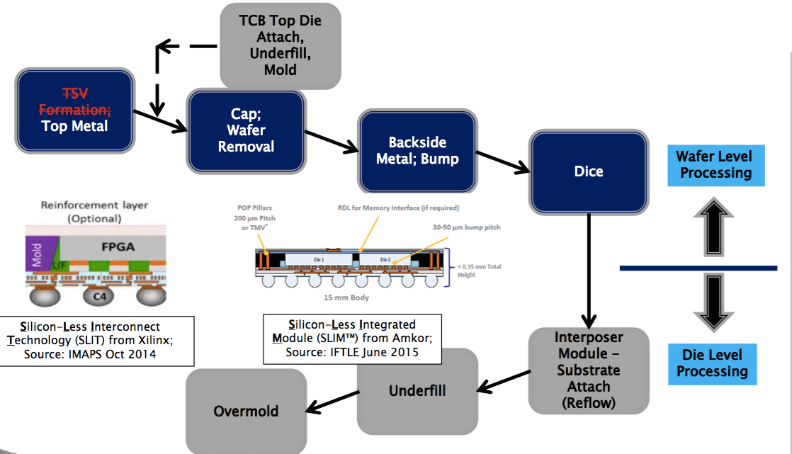
TSMC’s integrated fan-out (InFO) and integrated thin-film high-density organic package (i-THOP) from Shinko replace Si interposer with a build-up substrate and are potentially the lowest cost option. However line/space scalability below 2/2µm is a concern.
Lastly, Arkalgud talked about Invensas’ bond via array (BVA), a package on package (PoP) stacked approach for integrating logic and DRAM. BVA leverages the wire bond infrastructure to achieve high-density interconnects (up to 1600 I/0 count) and enables next-generation compact 3D component integration without the need for new equipment. BVA stacking technology was developed to bridge the gap between current packaging and emerging 2.5D/3D technologies
None of these options address cost of DRAM stacking. DDR4 DIMM (4 high, die to die) and the HBM/HMC (4+1 high, die to wafer) suffer from low throughput and UBM/ubump/underfill costs. One way to reduce cost for these 3D stacks is to eliminate costly processes, Arkalgud said. As an example, he talked about Ziptronix’ low-temperature direct bonding processes that can replace thermocompression bonding. I’ve written rather extensively about Ziptronix’ Zibond and direct bond interconnect (DBI) in the past, as its been a critical technology for 3D backside illuminated image sensors (BSI), which are now being manufactured in high volumes. Arkalgud showed how DBI compares with solder micro-bump bonding, as a low cost, better performing option that only lacks high-volume manufacturing proof points to become industry standard.
Arkalgud left us with some parting thoughts for the future of interposer integration and 3D stacking. Clearly, there is a vast array of options competing on cost that either leverage the existing infrastructure, eliminate TSVs, eliminate the interposer, eliminate process steps, or adopt wafer level processing. The winning platform technology will be stackable, scalable, possess good electrical and thermal characteristics, and be low cost. ~ FvT


