From March 16-20 the annual SEMI-THERM Conference (SEMI-THERM 2015) in San Jose gave me the opportunity to meet many assembly, materials, and thermal management experts. I also learned a lot about how IC packages and PCBs protect and cool single- and multi-die ICs. Both contribute significantly to cost, performance, and reliability of these designs.
Let me share with you my general impressions first, before talking about specific sessions. The variety of packages, the flexibility as well as the highly qualified technical experts I met, reminded me of my years in ASIC Marketing at VLSI Technology, 20+ years ago: No two ASICs were alike; differentiation and customer service were king; schedule- and cost pressure were enormous; and a portion of our designs never went into volume productions, therefor didn’t return the investments made.
In the last 20 years the application-specific standard product (ASSP) business model has replaced the ASIC model for many applications, especially due to lower unit cost, no NRE for users, and because “off-the-shelf” availability cuts risk. I am wondering if and how today’s high stress IC Packaging business model could be modified and, like the ASSP business model, bring benefits to both suppliers and customers in many markets?
Please don’t misunderstand: I am not dreaming of limiting packaging alternatives to something like the 8-24 pin DIPs we had 30+ years ago. I would like to initiate a discussion if and how modularity, best practices, and proactive efforts on all sides could bring benefits to all parties involved. Multi-die packaging, like PoP, SiP, interposer-based ICs, vertically-stacked dice in a 3D IC package, etc. only add complexity and multiply the opportunities for customizations. Should we start thinking about a lower risk, lower NRE, shorter time-to-market technology and business model now? It may also lower unit cost and increase margins for all companies contributing! Please share with us what YOU think about this!
Enough about the future, let’s look back at some highlights from SEMI-THERM 2015.
On Monday I chose – out of a range of Short Courses – Three-Dimensional Packaging: Manufacturing and Thermal Concern, presented by Jesse Galloway, Ph.D., Amkor Technology. Galloway started his talk with some basic information about electronic systems, IC design constraints and semiconductor ecosystem considerations. This made me realize that many packaging engineers have mechanical-, chemical- or other non-electronics degrees. That’s an important fact EDA vendors and IC developers need to consider when closely working with these experts in their fields.
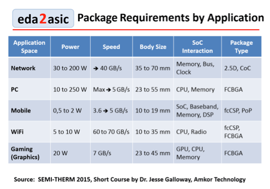
Galloway outlined the many assembly-steps, discussed the multitude of package types, and the different requirements of major applications. The table below shows a diverse range of package requirements. Galloway also outlined how board- and system-level simulations using Icepak or FloTHERM tools can avoid overheating and assure reliability during in-system operation. He pointed out that excessive temperatures during manufacturing can impact reliability significantly.
He confirmed the industry trend towards larger pin-counts as well as the need for much more bandwidths and higher I/O speeds. All of these suggest multi-die ICs as the principle solution. I really liked to hear this!
Tuesday morning’s keynote speaker was Chris Malone from Google. He manages Google’s (currently) 12 data centers and confirmed that even small data centers already consume tens of megawatts, or the equivalent of a small city, with 10,000s of homes. Power Usage Efficiency (PUE) is the key criteria for a data center. I also found interesting that he replaces server blades almost every year – to get more compute power while reducing electric power consumption – while his buildings and other infrastructure typically stays the same for decades.

Other speakers presented how they simulate, measure, and mitigate temperature problems in their specific application domains and clearly demonstrated that die-package-board co-design is essential for cost-effective ICs and systems. They also conveyed the need for accurate modeling of material characteristics and emphasized the importance of cooperation across the entire supply chain.
Overview of Thermal Challenges was the title of Dr. Herman Oprins tutorial from IMEC. His message focused on interposer and 3D IC designs and the R&D results IMEC has collected so far in this space. As usual, IMEC slides conveyed messages very clearly. The slide comparing different interposer materials especially caught my attention. IMEC’s Dr. Eric Beyne, the creator of this slide, gave me permission to share it with you. See below IMEC’s assessment of organic, glass and silicon interposers.
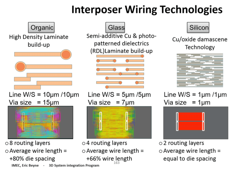
Please do not only look at the line width and spacing, presented in a very compelling way above, but also at the number of routing layers and interconnect lengths this specific design demanded, when implemented using different interposer materials. The slide clearly shows that, purely based on interconnect requirements, these three alternatives are quite different. Other considerations, like total IC power, I/O speeds, maximum on-chips frequencies and cost will of course narrow your options further.
Knowing Tom Tarter from many other packaging-related events, I skipped dinner on Wednesday evening to attend his presentation titled How to Select a Semiconductor Package. Tom compressed into a number of slides a very useful check-list for choosing the right package for your design. Tom’s slides, together with a number of other “How-To” presentations are available here. Last, but not least, on the exhibition floor I connected with a number of vendors, offering products and services in support of IC – package – board – system design as well as manufacturing. The full list is available in the Exhibitor Directory. ~ Herb