


TSMC 3D IC Reference Flows; A Leap Forward for the HMC
Big news for 3D ICs this week as TSMC and its OIP Ecosystem Partners announce the release of silicon-validated reference flows for both 3D IC stacks and 16nm FinFETS (everyone else puts the 16nm FinFETS first, but I’m most excited about the 3D IC news.) According to Peter Clarke in...
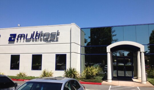
Multitest: Handling the Mobility Market
What better way to wrap up a busy week at SEMICON West 2013 than a site visit? After three days of interviews and PowerPoints, I was ready for some some hands-on demonstration. Barbara Loferer, marketing manager of Multitest, was concluding an open-house week at the company’s San Jose facility to promote...
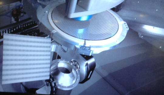
FormFactor Tackles Probe Test for 3D ICs
This is part of a series of short interviews, based on face-to-face meetings at SEMICON West 2013. For a long time, the jury was out on the probe-ability of micro-bumped TSV wafers. The jury was also unsure whether or not there was any point to probing to ensure known good...

SSEC’s New Chemistry for TSV Reveal
This is part of a series of short interviews, based on face-to-face meetings at SEMICON West 2013. SSEC had a lot to celebrate at this year’s SEMICON West, 2013. The company launched two new equipment platforms, WaferStorm and WaferEtch, each configuring single wet wafer processes for specific applications. Two of...

How will the 450mm Transition Affect Advanced Packaging and 3D ICs?
That was my kick-off question for Manish Ranjan, Vice President, Product Marketing, Advanced Packaging/Nanotechnology Segment at Ultratech, during our annual SEMICON West Thursday wrap-up discussion. It’s never been planned that way, but I always seem to interview Ranjan at the tail-end of SEMICON West, and subsequently end up bouncing a...
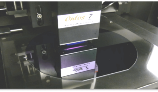
SETNA: Atmospheric Plasma Surface Modification
This is part of a series of short interviews, based on face-to-face meetings at SEMICON West 2013. SET is known in the 3D IC world for its high accuracy die bonder for die-to-die and die-to-wafer stacking. The SET Representative in North America (SETNA) has also launched a companion tool, ONTOS7,...
EV Group: Never a Dull Moment
This is part of a series of short interviews, based on face-to-face meetings at SEMICON West 2013. Sitting down with EV Group execs to talk about the company’s latest achievements and contributions to the 3D IC cause has become an annual SEMICON West tradition. In fact, I’ve probably spent more...
NORDSON: Newcomers to 3D ICs
This is part of a series of short interviews, based on face-to-face meetings at SEMICON West 2013. As 3D ICs get closer to volume manufacturing, we’re seeing newcomers joining the 3D IC party with solutions that help along established process flows, and fill in gaps. Longtime suppliers to the mainstream...

Silicon Photonics: the Next Killer App for 3D ICs? and more from the R&D Community
First it was going to be memory stacks, then it was Wide I/O DRAM on Memory, and now, as commercialization of 3D ICs gets pushed out further, will it be Silicon Photonics that drives 3D ICs to volume manufacturing? That was the opinion expressed by Michael Liehr, executive VP of...
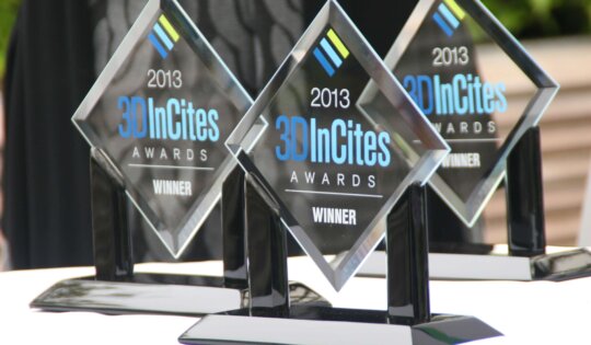
And a Good Time was had by All – 3D InCites Awards Breakfast, 2013
Despite the chilly San Francisco morning temperatures, a sizable crowd of 2.5D and 3D enthusiasts gathered at the Impress Lounge to witness the inaugural 3D InCites Awards Breakfast, held July 11, 2013 during SEMICON West. For me, it was especially significant as it marked four years since I first launched...
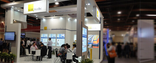
2013 SUSS MicroTec Technology Forum Focuses on 3D TSV infrastructure
SUSS, being an equipment maker addressing various manufacturing challenges faced by 3D IC enablement, definitely has a lot riding on ensuring that all pieces of the 3D IC puzzle are in place. This was evident from the range of presenters they had lined up during this year’s Technology Forum, held...

Late Breaking SEMICON West News: Expert TechHUBs Added to this Year’s Agenda
New this year at SEMICON West, and just introduced to the program late last week, the Expert TechHUBs will help attendees find answers to specific semiconductor test and packaging questions. Meet with industry experts in an informal discussion group on the North Hall show floor at TechHUB Test or in...

Semi Trade Pubs Talk 3D, Just in time for SEMICON West
That Jan Vardaman, she’s so clever! I just finished reading her column on ECTC 2013 in Printed Circuit Design and Fab, and thought her quippy, Las Vegas-y references in the opening paragraph were right on the money. Vardaman’s take on ECTC was similar to my own, discussed here in my...

Momentum Builds for the 2013 3D InCites Awards
Subscribers are practically blowing up 3D InCites as they duke it out online and race the July 3rd deadline for casting their ballots in the public opinion poll for this inaugural 3D InCites Awards; which is great because the first 3D InCites Awards Breakfast, co-presented by 3D InCites and TechSearch...

EV Group Enhances Wafer Debonding Solutions Portfolio with New LowTemp Room-Temperature Debonding Platform
Three high-volume-production room-temperature debonding process types are supported by a supply chain of seven qualified adhesive suppliers to enable greater manufacturing flexibility St. Florian, Austria, July 1, 2013 — EV Group (EVG), a leading supplier of wafer bonding and lithography equipment for the MEMS, nanotechnology and semiconductor markets, today introduced...
3D Buzz from ConFab, 3D Integration at IITC 2013, and more
So SPIL’s offering a turnkey model for 2.5D interposers, including fine-pitch fabrication of the interposer wafers themselves? This is certainly an interesting turn of events, particularly with TSMC’s recent announcement that they’re not married to the turnkey model and are willing to collaborate with OSATS. SST’s Phil Garrou got the...
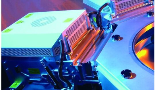
SPTS: ReVia Endpoint System
Product Description ReVia is a new endpoint detection (EPD) technique that can monitor the progress of “via reveal” etch processes even at remarkably low (<0.01%) via densities. It is a unique solution that can significantly increase yields for device manufacturers involved in emerging 3D packaging applications utilizing through-silicon vias (TSVs)....
SSEC: 3300 Series for TSV Clean
Product Description: Post DRIE etch TSV cleaning is essential to the reliability of 2.5D and 3D IC devices. SSEC’s proprietary soak and spray technology minimizes spray time and chemistry use for lower cost-of-ownership than conventional wet bench or single spray approaches; it achieved 100% photoresist and sidewall fluoropolymer removal 5x...
Technology Updates at ECTC 2013
The ECTC 2013 stats are in. This year showed increases across the board with: Over 1,300 attendees, the highest attendance ever, from 26 countries 377 technical papers, presented in 36 oral and five interactive presentation sessions, including a student poster session 12 sessions focused on 3D/TSV, including several of the...
ECTC 2013 Interview: SPTS’s Keith Buchanan Addresses Bow and Warp
A few weeks ago I spoke with SPTS’s David Butler, after he participated in the SEMICON Singapore 3D IC panel. We talked a lot about the importance of wafer planarity for performing backside processes like TSV reveal. Butler commented that regardless of a tool’s calibrated precision, its only as good...