This is part of a series of short interviews, based on face-to-face meetings at SEMICON West 2013.
As 3D ICs get closer to volume manufacturing, we’re seeing newcomers joining the 3D IC party with solutions that help along established process flows, and fill in gaps. Longtime suppliers to the mainstream advanced packaging market, NORDSON Dage and NORDSON March, have each identified areas in 3D IC manufacturing that benefit from their core competencies, and are working with customers to fully develop these tools and processes. I spoke with representatives of both divisions to learn more.
Evstatin Krastev, International Applications Engineering Manager, NORDSON Dage, and David Bernard, Business Manager for NORDSON Dage Automated X-ray Systems, clued me in on the companies activities in developing an X-ray system for TSVs.
As silicon is transparent by nature, up until now, X-ray has not been an effective method of wafer inspection. But with TSV metallization, it’s proving to be a more effective way of finding voids in TSV fill than FIB or SEM photography. X-ray is a non-destructive test and can be performed on the whole wafer. Krastev talked about the companies tool, NORDSON Dage Diamond, which he says can check for voids down to 100nm resolution (1µm). As aspect ratios of vias get smaller, the best possible X-ray tool is needed, he said. Dage has been working for almost 3 years on TSV inspection technology.
Bernard explained that the company wanted to offer a more practical solution for Foundries and OSATS for TSV and wafer bump inspection. X-ray is a new technique in the semiconductor middle end, he explained. Not only can it detect voids in TSVs, but in bumps as well. Expect to hear more on this from Dage in the near future.

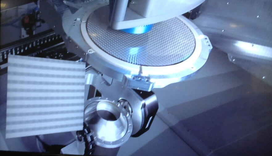
I’ve been hearing more about the importance of cleaning processes TSVs and 3D IC stacking lately, and have focused mainly on wet processes for TSV clean. NORDSON March has been working on a different approach: dry clean processes using plasma. Jonathan Doan, Director of Marketing for NORDSON March, said that the company has been working with industry partners to develop plasmas for polymer removal for TSV clean, and also oxide removal for copper pillars and pads. He said the importance of removing oxide and copper contamination post backside thinning and prior to bonding is critical to forming a strong bond.
The benefits of plasma processes over wet processes, according to Doan, include cost saving by replacing wet chemistry, better uniformity control and throughput.
He also said that when it comes to high aspect ratio (HAR) TSVs, wet clean prcesses are limited on penetration, where plasma processes can get to it. So for TSVs, the company is focusing on HAR. A number of companies have expressed interest in the technology and are running in-house samples, and Doan says March is working with research partners on an aggressive roadmap, and hope to introduce the tool in early 2014. ~ F.v.T.