
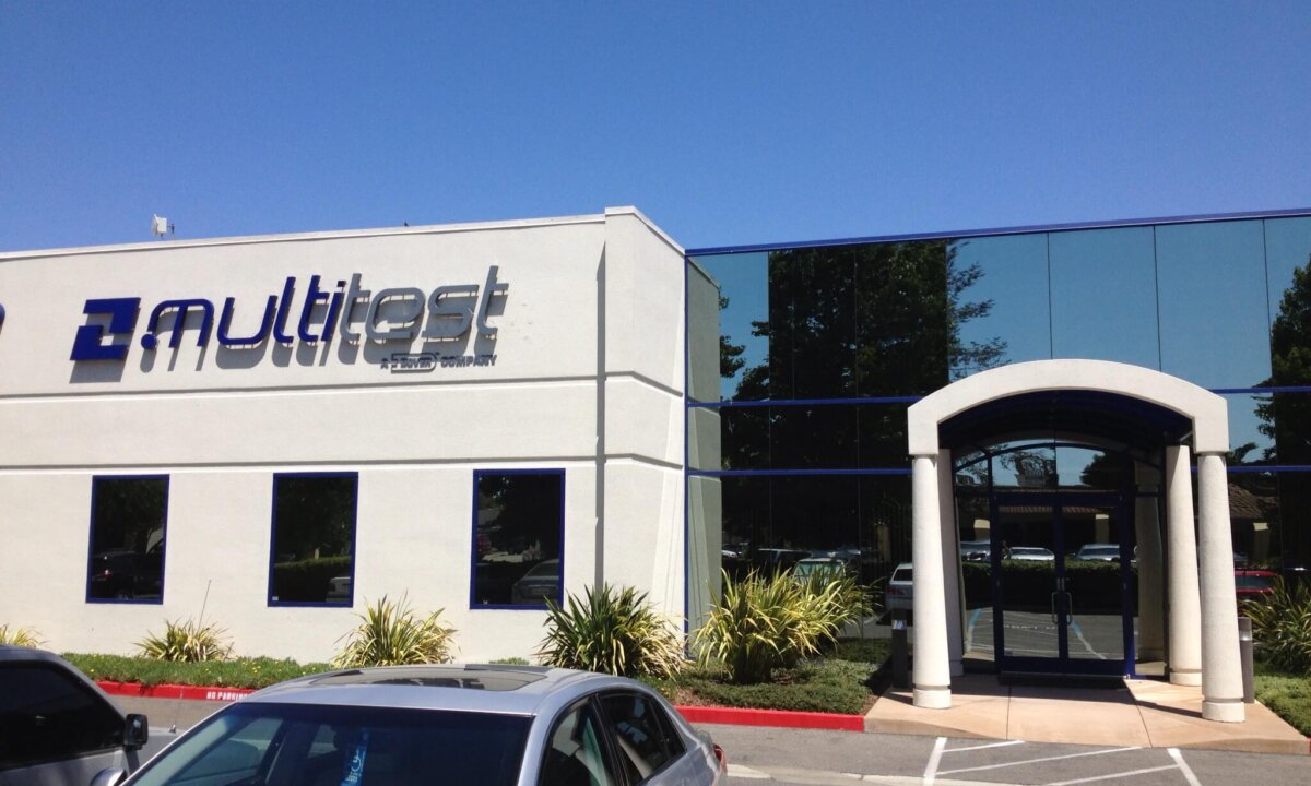
What better way to wrap up a busy week at SEMICON West 2013 than a site visit? After three days of interviews and PowerPoints, I was ready for some some hands-on demonstration. Barbara Loferer, marketing manager of Multitest, was concluding an open-house week at the company’s San Jose facility to promote the company’s current focus on the mobility market and subsequent product enhancements, and she invited me to visit and see first-hand Multitest’s Plug ‘n’ Yield philosophy in action.
My visit began with an overview briefing by Loferer, who explained how Multitest’s product offerings support semiconductor test at 3 levels: wafer level, in-process and final test. With a strong legacy in automotive electronics, including MEMS and sensors, the company is leveraging its core competencies, which include test handlers, contactors and load boards, into integrated solutions that match global trends in micro- and nano-electronics including the “internet of things (IoT)”, mobility and connectivity, and ecology and sustainability.
The Multitest of today comprises the product lines of three companies merged into one; Harbor Electronics, manufacturer of load boards; Everett Charles Technologies (ECT) contactors, and the original Multitest, handlers. They all came together under the Dover umbrella. The company considers itself to offer “best in breed” in each individual product area. “We are tying to provide an integrated solution to our customers,” explained Jim Quinn, VP Marketing, “No other company has this combined portfolio. It’s a natural fit for sensors and 3D ICs.”
Who are Multitest customers? OEMS and IDMs, Foundries and OSATs, of course. Fabless companies are also considered to be target customers, explained Loferer, because they drive decisions. Probe card manufacturers such as MicroProbe and Formfactor are also customers, as they buy load boards. The only element of test that’s not in Multitest’s portfolio is the testers themselves. They work with companies like Teradyne, LTX and Advantest to provide handlers for leading-edge test technologies that meet customer needs matched with global trends. These days, that means matching requirements of the mobility market with production.
“For Multitest it is a new approach to systematically consider trends of the electronics end markets and not just be customer driven, developing products for individual customers,” noted Loferer.
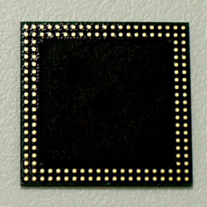
To this end, the company has thoroughly done its homework. They’ve consulted with market research firm, Prismark Partners, to validate package trends. They’re looking at mobile devices and how they will develop; for example, which packages and IC devices inside tablets require test. Chip scale packages are “a big deal” as are package-on-package (PoP) devices. In four to five years, it will be TSV stacks.
Keeping up with market trends and supporting them in high volume means providing the highest parallel test with the highest throughput and low jam rates. Contactors need to have long lifespans and cleaning cycles with high first-pass yield, and load boards need to have high layer counts to support the high parallel test. “In high volume manufacturing, test shouldn’t be the bottleneck,” said Loferer.
Supporting highly integrated, high-density packages calls requires load boards, contactors and handlers to work in concert to allow for more contactors with low force probes. High-density devices heat up faster and hotter than other devices, and can cause false test results, creating yield issues.
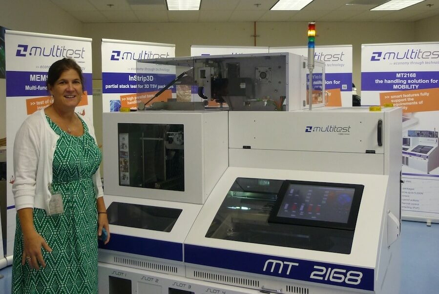 My visit also included a demo of the company’s newest handling solution, the MT2168, which has been equipped with “smart features for mobility” including active thermal control (ATC) and double sided contacting to test PoPs. Guenther Jeserer, business unit manager for gravity and pick and place, Multitest, showed me around the tool, pointing out the unique features that set it apart from other handlers. He explained that the tool operates “ambient hot”, which means room temperature up to 155°C. Additionally, the ATC capability allows for handling stacked die packages that require more heat dissipation due to self-heating. Jeserer showed me how the plunger is fitted with a metal heat sink to keep the air around the die stack cooler than the test temperature to keep it stable.
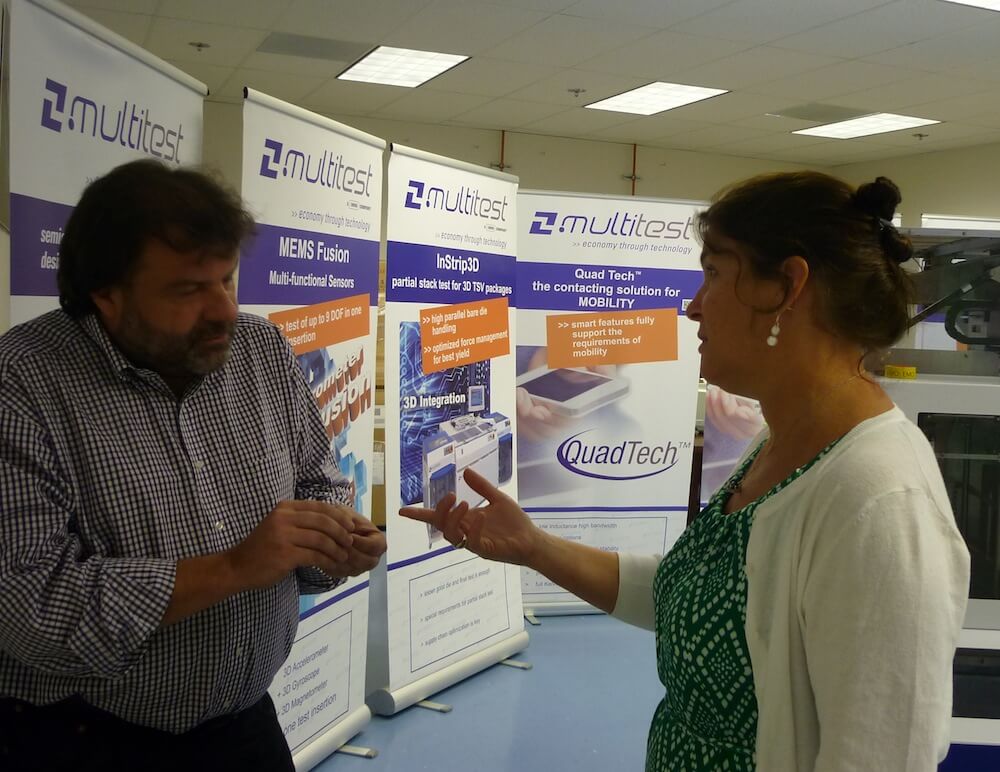
 For PoPs, testing of the bottom package is a real challenge, because it is unique from standard packages in that it requires testing on the top and bottom. Jeserer showed me the double-sided contactor that simultaneously tests both sides of a PoP.

For highest throughput, the handler supports testing of up to 32 devices simultaneously. It has a 3-headed plunger assembly that features multiple handling steps in parallel , rather than using serial approach like the competitors. A “soak wheel” ensures adequate temperature “soak” capacity.
When connected to the tester, devices can be sorted into different bins by category, based on requirements. Jeserer said up to 32 categories can be assigned for sorting tested devices.
After the demo, I sat down with Jim Quinn; Reinhart Richter, President, Multitest; and Tim McNulty VP Interface Products; to talk more specifically about how 3D IC and TSVs play into all of this.
While testing PoP may be more complicated due to the dual-sided nature of the bottom package, final testing TSV stacks isn’t much different than testing a single die package with regards to contacting and power dissipation. However it is more fragile and shock sensitive, and requires handlers with a ‘soft’ plunge.
In 2.5D and 3D IC testing, probe is a hot topic, and spring probe pins are a hallmark of Multitest’s interface division. McNulty explained about the next generation view of spring probes. They will have sharp tips for oxide penetration and deliver low force. The penetration of oxide has to be efficient, he said.
3D stacking processes are more intricate than pure assembly, noted Richter. 2 or 3 die in a 3D stack requires an elaborate tester to do full functional test, which isn’t very economical. Built-in self-test adds cost and takes real estate. “Going to 3D means re-thinking the test strategy from what it was in the past,” explained Richter, “Final test can’t be the same final test. We need to move more towards in-line test and functional test, which is faster.” Part of Multitest’ 3D solution is its partial stack test, which I learned about at ECTC 2013.
One of many takeaways from my visit to Multitest is how in developing the handlers, contactors, and boards, there is more thought given to how the parts interact to provide a complete and robust solutions than their would be if each division was a stand-alone company. Load board wear and tear matters, as does the lifespan of the contactors. “Handlers have to apply force, and contactors have to be capable of taking that force and routing out,” Quinn explained. “Customers can source from different suppliers, but then they have to figure out how to integrate this. Do they really want their engineers to worry about that when they can let us focus on the integration?” That’s what plug and yield means.
At the end of the day, Multitest is unique due to the sum of its parts. The plug and yield philosophy is intended to deliver the message to customers, “you worry about your devices, and leave the handling to us.” And it does. ~ F.v.T.


