
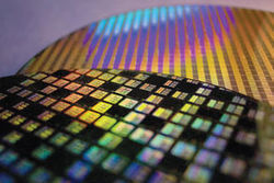
So SPIL’s offering a turnkey model for 2.5D interposers, including fine-pitch fabrication of the interposer wafers themselves? This is certainly an interesting turn of events, particularly with TSMC’s recent announcement that they’re not married to the turnkey model and are willing to collaborate with OSATS. SST’s Phil Garrou got the scoop this week from SPIL’s Mike Ma, at the Confab.
Reporting back from this year’s IITC 2013, held in Kyoto Japan June 13-15, 2013, Rambus’ Deepak Sekar and IBM’s Vincent McGahay contributed a technology round-up on interconnect challenges that was published here in Solid State Technology. In the 3D integration segment, the authors note that papers in this area reflect a trend that 3D is “moving from concept to implementation phase.” They summarize a paper by Ho-Young Son from Hynix, who honed in on stress to transistors caused by TSVs. Son says the company has had success in optimizing processes to achieve reliability. Also of interest, 3D stacking has made it into Tohuku Univerisity’s prototypes for Spin-Transfer Torque MRAM (STT-MRAM). The prototypes reportedly comprise 90nm CMOS technology as well as 2232 TSVs and microbumps.
Thermal issues in 3D ICs is one of the remaining technical issues for 3D IC adoption. iMicronews recently devoted one of its “closer look” pieces to IBM’s work developing a test vehicle to address thermal resistance in 3D chip stacks. The experiment measured temperature at various levels in the chip stack. They found that lower chips in the stack are hotter, presumably because they are farther from the heatsink. The researchers surmised that higher temperatures in a zone are believed to be due to variations in the thickness of the TIM layer. The temperature difference between adjacent chips increases as the pitch of the microbumps is increased. More findings are reported here in the full story.
Other 3D IC related tidbits that I found interesting include an announcement by Austrian chip maker, AMS, that they will integrate through-silicon via (TSV) 3D IC fabrication technology into its ambient light sensor devices for use in smartphones and cameras.
Earlier this spring, nVidia announced its next GPU Family, Volta, will use TSVs to interconnect stacked DRAM to the GPU. Target release date: 2016. Yes indeed, the implementation phase is firmly upon us. Won’t be long now. ~ F.v.T.


I don’t think the TSMC foundry turnkey model and SPIL OSAT turnkey model should be put together to discuss, they are very different in context.
Each company in a supply chain like to do more, provided capability allowed, to increase its added value (in the form of revenue, profit, market share..). However, when the role of one company growing to be dominant and near no competition, market (customer) would concern the risks of loosing control and lack of bargain power, no place to go to except one. In either 2.5D or 3DIC, TSMC can do everyting, except the memory wafers, all by itself. So they gave out the work of mounting finshed chip and Si interposer module to laminated substrate, so this counting what 3% of the total value? So, their role in 2.5DIC going down from like 85% (15% for not making DRAM wafers) to 82%, still quite dominant.
On the other hand, SPIL don’t manufacture IC wafers, they just do microbumping of IC wafers, they did Si backside with foundry, and all the assembly work. So they now move to front side of Si interposer including TSV and can complete the entire Si interposer, in the same analogy, their role probably going up from 20% to 30%? I would consider this post little concern as their service can still be manageable, still can be leveraged by other OSAT foundry combination (Amkor or STATSChipPac plus Global Foundries, ASE+UMC, etc), and TSMC is still there. Move over, the customer can leverage with their exisiting businss with OSAT, and OSAT has no foundry rival who happen to be the biggest DRAM supplier in the market. If this work, other OSAT can also follow its foot steps and this make the supply chain ‘abundant’ this is what market would like to see.
As a previos post at ECTC panel, whatever the business model is, at the end, market (who pay the money) decide who they want to work with.
GHMMA – Thank you for this perspective. I see your point and agree. A manufacturing company’s goal (whether foundry or OSAT) is to develop their own strategies to leverage their core competency, deliver product and gain as market share as they can. The overall benefit to the industry is a more robust supply chain over all, offering options to customers. In the end, the customer decides.