

Three high-volume-production room-temperature debonding process types are supported by a supply chain of seven qualified adhesive suppliers to enable greater manufacturing flexibility
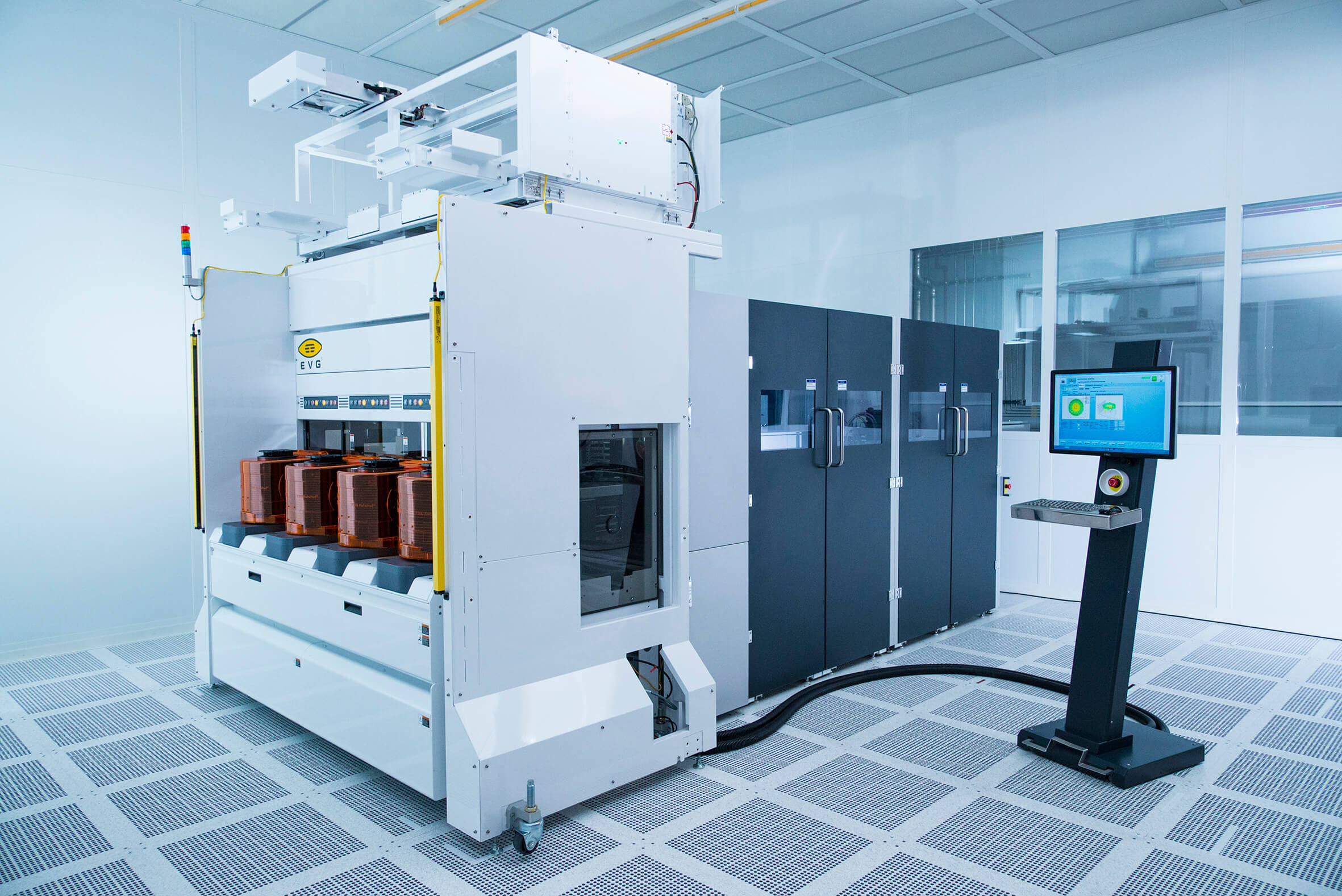
St. Florian, Austria, July 1, 2013 — EV Group (EVG), a leading supplier of wafer bonding and lithography equipment for the MEMS, nanotechnology and semiconductor markets, today introduced its LowTemp™ debonding platform, which features three different room-temperature wafer-debonding processes and an extended material supply chain. The platform includes two new debonding processes that have been qualified for EVG’s high-volume production temporary bonding/debonding (TB/DB) systems—UV laser debonding and multilayer adhesive debonding—in addition to EVG’s ZoneBOND® technology, which has already been implemented into production across the compound semiconductor and advanced packaging markets. EVG’s LowTemp debonding platform is complemented by a supply chain of seven material suppliers, with a wide choice of qualified adhesives that support a variety of bonding applications and offer greater process flexibility for customers.
“For more than 15 years, EVG has provided leading-edge temporary bonding and debonding solutions to our customers,” commented Paul Lindner, EVG’s executive technology director. “The experience and know-how that we’ve built up from our numerous installations in high-volume manufacturing has taught us that one solution doesn’t fit all applications when it comes to temporary bonding/debonding. Accordingly, EVG offers highly flexible and modular equipment, a wide choice of qualified materials to support customers’ individual requirements and multiple source policies, and process development and implementation support through our worldwide application labs and cleanroom infrastructure across a range of applications—including interposers, stacked memory, memory on logic, power devices and compound semiconductors.”
EVG’s LowTemp debonding platform adds to the company’s already comprehensive portfolio of temporary bonding/debonding and thin-wafer handling solutions based on tape debonding and thermal slide-off debonding technology. The LowTemp debonding platform is available on EVG’s full line-up of TB/DB systems, including the recently announced EVG850TB/DB XT Frame high-volume production platform, which can achieve a throughput of more than 40 wafer stacks per hour and features an optional, integrated in-line metrology module that takes up to 300,000 measurement points at unprecedented speeds to enable real-time monitoring of the bonding/debonding process for maximum yields.
About EV Group (EVG)

EV Group (EVG) is a leading supplier of equipment and process solutions for the manufacture of semiconductors, microelectromechanical systems (MEMS), compound semiconductors and power devices, and nanotechnology devices. Key products include wafer bonding, thin-wafer processing, lithography/nanoimprint lithography (NIL) and metrology equipment, as well as photoresist coaters, cleaners and inspection systems. Founded in 1980, EV Group services and supports an elaborate network of global customers and partners all over the world. More information about EVG is available at www.EVGroup.com.


