

EV Group News - Page 2
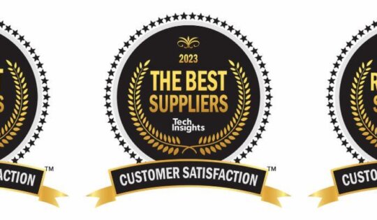
EV Group Scores Big with Eleventh Consecutive Triple Crown Win in TechInsights 2023 Customer Satisfaction Survey
EVG achieves its highest rankings ever with 5 Star ratings across all applicable award categories; continues winning streak with 21st...
EV Group and Dymek Company Form Joint Venture Company in Malaysia to Enhance Regional Customer Support
EV Group (EVG), a leading supplier of wafer bonding and lithography equipment for the MEMS, nanotechnology and semiconductor markets, and...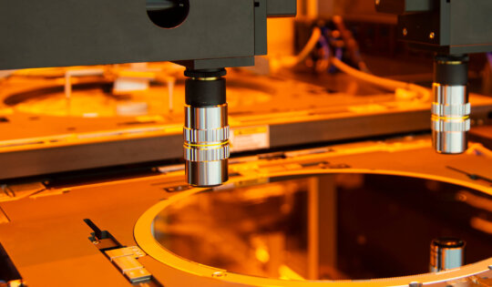
EV Group Solutions for Heterogeneous Integration to be Highlighted at ECTC 2023
Papers to highlight breakthrough capabilities of EVG’s hybrid bonding, LITHOSCALE® maskless lithography and NanoCleave™ layer release technology for advanced packaging...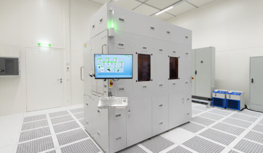
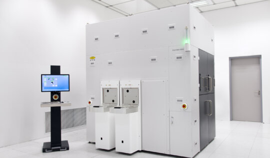
EV Group Advances Leadership in Optical Lithography With Next-Generation EVG150 Resist Processing Platform
ST. FLORIAN, Austria, November 7, 2022—EV Group (EVG), a leading provider of wafer bonding and lithography equipment for the MEMS,...EV Group Revolutionizes 3D Integration from Advanced Packaging to Transistor Scaling with NanoCleave Layer Release Technology
IR laser cleave technology enables nanometer-precision layer transfer through silicon, eliminating glass substrates for advanced packaging and enabling thin-layer 3D...
EV Group Expands Collaboration with ITRI on Heterogeneous Integration Process Development
ST. FLORIAN, Austria, August 30, 2022—EV Group (EVG), a leading supplier of wafer bonding and lithography equipment for the MEMS,...
EV Group Achieves Die-to-Wafer Fusion and Hybrid Bonding Milestone with 100-Percent Die Transfer Yield on Multi-Die 3D System-on-a-Chip
Successful full-system die-to-wafer transfer at EVG’s Heterogeneous Integration Competence Center™ demonstrates an important step forward in process maturity EV Group...
EV Group Earns Outstanding 10th Consecutive Triple Crown Win in TechInsights 2022 Customer Satisfaction Survey
EVG achieves 5 Star rating for first time in both “10 BEST” and “THE BEST” suppliers segments; continues winning streak...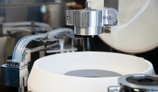
EV Group Lithography Solutions for Heterogeneous Integration and Wafer-level Packaging to Be Highlighted at ECTC 2022
Technical papers to highlight the breakthrough capabilities of EVG’s LITHOSCALE® maskless lithography solution and OmniSpray® resist coating technology for “More...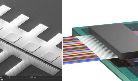
EV Group and Teramount Announce Collaboration to Implement Innovative Packaging Technologies for Photonic Integrated Circuits
Breakthrough wafer-level optics technologies help solve a key challenge of connecting many fibers to silicon chips for datacom and telecom...EV Group Recognized by Bosch as a Preferred Supplier of Semiconductor Equipment
EVG is the first semiconductor equipment supplier ever to receive Preferred Supplier status EV Group (EVG), a leading supplier of...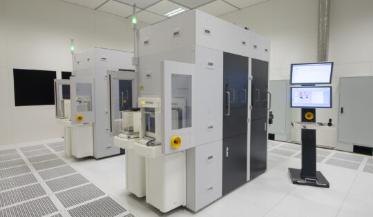
New Multi-Functional Micro- and Nanoimprint Solution from EV Group Offers Unprecedented Flexibility for High-Volume Optical Device Manufacturing
ST. FLORIAN, Austria, January 18, 2022—EV Group (EVG), a leading supplier of wafer bonding and lithography equipment for the MEMS,...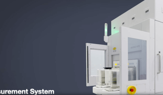
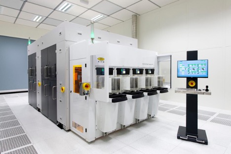
EV Group Brings High-speed High-precision Metrology to 3D Heterogeneous Integration
EVG®40 NT2 offers breakthrough metrology performance to accelerate implementation of wafer- and die-level hybrid bonding and maskless lithography FLORIAN, Austria,...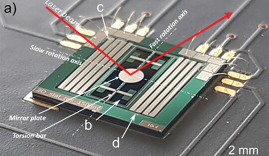
Cooperation of ZKW Group with Silicon Austrian Labs, Evatec, EV Group and TDK Electronics advances light projection technology
WIESELBURG, Austria, August 25, 2021—Together with research partners Silicon Austrian Labs, Evatec, EV Group and TDK Electronics, ZKW is working...
EV Group Launches First-of-its-Kind Step-and-Repeat Mastering Services for Nanoimprint Lithography
EVG S&R Mastering Shop™ further lowers barriers to adoption of nanoimprint lithography for wafer-level and panel-level production applications such as...
EV Group Unlocks Agile and Efficient Production Scaling with Next-Generation Step-and-Repeat Nanoimprint Lithography System
EVG®770 NT enables large-area master stamp fabrication of complex micro- and nano-structures for augmented reality waveguides, wafer-level optics and advanced...ASM Pacific Technology and EV Group Join Forces to Enable Industry’s First Ultra Precision Die-to-Wafer Hybrid Bonding Solutions for 3D-IC Heterogeneous Integration
Joint Development Program will offer highly configurable, ultra-precision end-to-end hybrid bonding solutions to suit various applications, with optimal line balancing...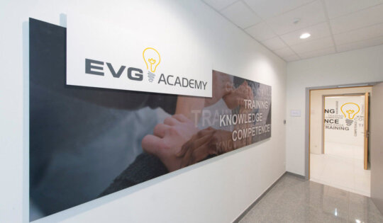
EV Group Establishes State-of-the-Art Customer Training Facility at Corporate Headquarters
EVG Academy doubles the amount of training space and technical trainers; provides training on every class of EVG equipment and...