


Alchimer’s latest technology breakthrough is an interesting twist on the way semiconductor solutions generally presents themselves. We’re used to hearing about scaling that goes from bigger to smaller. This is the first time I’ve heard of a technology that scales UP to meet application needs. But that’s precisely the differentiation between Alchimer’s flagship suite of wet deposition processes, the AquiVia line, and its latest product introduction, AquiVantage. While the AquiVia line works on the vertical to molecularly grow nanoscale films, AquiVantage works on the horizontal to grow microscale films. “We’re talking 1-5µm as opposed to 50-200nm thick,” notes Steve Lerner, CEO, Alchimer, “using the same processes, same tools, and materials; it’s just a different application.”
Lerner explains why: because Alchimer’s process molecularly grows structures to create nanometric films, rather than depositing materials that then need to be etched or polished away. AquiVia, targets TSV metallization processes including barrier, seed, isolation, and fill steps. AquiVantage is suited to via last backside metallization processes, such as isolation, redistribution layer (RDL), and under bump metallization (UBM). “Basically, now we can offer everything short of the bumps themselves,” he says.
Lerner explained that traditional backside metallization processes begin with spin coating a material like BCB or some other polyimide, then areas that need to be microbumped and connected to the RDL are selectively etched away using a mask step. In the AquiVantage process, the wafer is put in the electrodeposition (ECD) chuck, making contact around its periphery. Then, the isolation layer is grown out from the surface selectively. Because vias are filled and already surrounded by isolation and barrier, there’s no electrical charge that allows film to grow on them. Rather than patterning the film, it’s being selectively grown, and the need for patterning is eliminated. Lerner says the properties of AquiVantage isolation save the customer an entire mask step; roughly 30% of the cost of backside metallization process, it’s huge.
The most interesting application opportunity for both the AquiVia and AquiVantage processes to be used together is in silicon interposers. “With interposer we can simultaneously grow the TSV stack and the horizontal metallization,” notes Lerner. “Provided that you can balance the thickness, isolation can be grown in the via as well as on top.” Add that to barrier and fill steps and you can eliminate 8 steps from the 27-step interposer process flow (Figure 1). “It’s a huge savings,” notes Lerner.
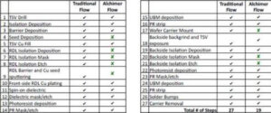
Figure 1. The Alchimer flow eliminates 8 steps out of 27, i.e. a process flow reduction of 30%.
Lerner said that AquiVia films were designed for nanometric ranges, and could achieve a maximum thickness of .5µm, such as required for dual damascene/TSV range of dimension. “One film couldn’t get much thicker and still maintain its structural integrity,” he explained, “so we hadn’t branched out into other applications. But when this capability appeared, it unlocked a whole bunch of doors, it was a chain reaction.”

Lerner says Alchimer has always seen itself as being very applicable to interposer processes because its one of those areas that will be extremely cost competitive, it’s far less critical than handling expensive wafers, and offers a huge value to the OSATs. “I personally believe that interposer is going to be not only our catalyst, but that of the industry as a whole,” predicts Lerner. “While everyone is waiting for (TSV) standards, some innovative people are going to come in and do interposer to capture certain products like Xilinx/TSMC did. We’re all super excited about this.” He added that the interposer is going to be like another package; silicon BGA, if you will. There’s much less liability involved and it will give people a lot freedom. “They can wring out all the bugs in the TSV process, and then they can go back and work on via-mid processes, which are incredibly more complicated,” he explained.
The AquiVantage breakthrough happened about a month ago, and coupled with fill gives the company a toolbox to do just about everything using one single tool. ”You don’t need a CMP or PVD tool; or half of what’s needed for constructing interposers using dry processes.” Lerner says he believes the OSATs stand to gain the most from this technology, as well as those providing bumping services. In fact, he predicts that bumping houses are going to go into the interposer business, because it’s so aligned with their core business. “All they need to do is add a DRIE tool, and the infrastructure is there to put them in the high-end substrate business,” he says.
“The savings are stark,” Lerner notes. “This is much, much bigger than just a TSV and for us as a company it’s exciting because it applies to real revenue-generating segments of the industry. Everybody’s waiting for the TSV to get pregnant….next year, the year after….well this is going on right now in volume. Customers have encouraged us to move in this direction,” he says. “It (interposer) is more in demand than TSV, so that’s why it’s a welcome breakthrough. It’s a here-and-now application. TSV is yet to explode; this is mainstream stuff.”


