


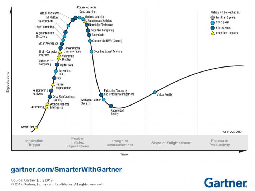
Long gone are the days of the “killer app” and the notion that a single device market like personal computers (PCs) or smartphones alone can make or break the semiconductor industry. In fact, while both those markets have softened, a multitude of emerging technologies including 5G, artificial intelligence (AI), internet of things (IoT) platforms, deep learning, autonomous vehicles, blockchain and many more are marching up and over the Gartner Hype cycle’s curve to keep the industry humming along (Figure 1). Semiconductor device manufacturing requirements are as varied as the applications themselves, as are the ways to integrated and package them. Fan-out (FO) packaging platforms are popping up all over the place in many varieties to address this ever-broadening application landscape. In an attempt to better understand this elusive market space, we talked to Ron Huemoeller, Corporate VP and Head of R&D at Amkor Technology Inc., winners of the 2018 3D Incites Award for Device Manufacturer of the Year.
Fan-out Market Drivers
Despite the clear slowdown, Huemoeller says, smartphones are still the main driver of fan-out technologies, primarily due to form factor and cost benefits. Fan out packages are currently employed from the microprocessors to the power management ICs (PMICS), radio frequency (RF) transceiver devices and CODEC devices for rapid data transfer. Other key end-markets now pursuing fan out packaged products include networking, AI, 5G and automotive electronics.
Huemoeller says fan out technology drivers are predominately cost, package profile and electrical performance. For example, WLCSP packaged silicon at lower nodes is shifting to FO to harvest the benefits of lower cost due to die shrink while maintaining the same ball out footprint, as well as a thinner profile.
Additionally, in the microelectromechanical systems (MEMS) space, FO enables sensor fusion, thereby addressing sensing needs for industrial and automotive applications. In fact, 3D MEMS FO solutions are already entering the market. By using advanced RDL lithography on films, die can be linked at the wafer level and molded to create mini-modules that can be integrated onto other substrate media.
“At the advanced product end of our market, a solution that lowers cost and improves electrical performance can be derived by using high-density fan out (HDFO), in combination with traditional substrate technology,” said Huemoeller. “Ultimately, an HDFO module on the substrate is formed, bringing together the premier aspects of each technology.”
Understanding the FO Hierarchy
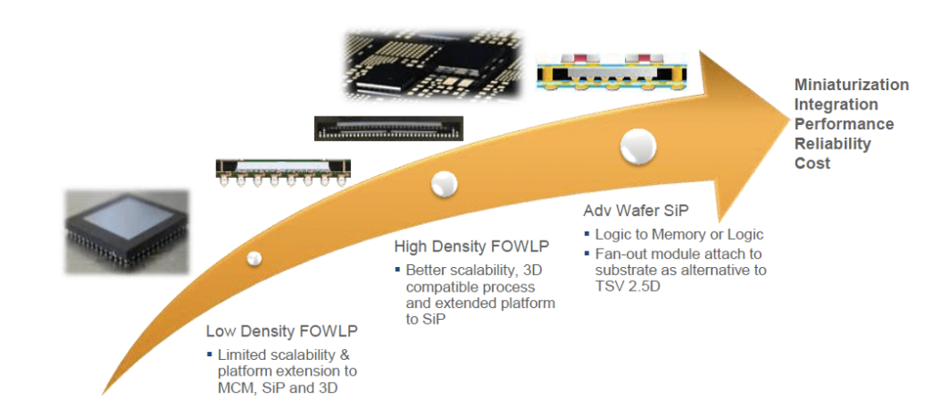
Ranging from the traditional single die, embedded wafer level ball grid array (eWLB), to system-in-package (SiP) mini-modules, to 3D FO, there are, according to Huemoeller, “literally dozens of versions of fan-out today.” Furthermore, the introduction of 3D FO has generated a myriad of creative connectivity approaches (Figure 2).
Luckily, all of them can be categorized under two headings: low-density fan-out (LDFO) and high-density fan-out (HDFO). Huemoeller explained that there is a clear division of these two markets in approach and support.
“LDFO extends in many product applications due to its unique ability to address form factor and density through lithography reduction over substrates. It sufficiently addresses the mobile market for PMIC, RFIC, and CODEC,” he explained. “HDFO, due to cost and complexity, is targeted at higher value die and applications, where interactive functionality at a much higher level is required.” Unlike the LDFO path, whether face up or face down, there are only two ways to approach this today and still achieve all the electrical and reliability requirements.
FO vs. The Alternatives
To complicate things further, there are other approaches to packaging that are vying for the same applications, particularly in high-performance computing, where cost is less of a deal breaker. These include 3D through silicon vias (TSVs) and interposer integration approaches. “There are many ways to generate die to die connectivity,” noted Huemoeller “The optimal approach will be the lowest cost, highest yielding solution.”
For example, the much-talked-about “chiplet” approach for partitioning silicon and integrating functional IP blocks onto a substrate (Si or organic) appear to be very similar to the FO SiP mini-modules Huemoeller describes. The main differentiator is the lithography line/space limitations. Chiplets on a Si substrate can achieve <1µm l/s, while HDFO is limited to just under 2µm l/s. The chiplet approach on a single silicon substrate, however, is expensive and has supply chain limitations. One of the more complicated, but elegant methods being developed today incorporates the use of Si “bridges” to provide die-to-die connectivity and helps to address the cost at the same time.
“The chiplet approach addresses the complexity we see in SoCs today,” said Huemoeller. “We can’t continue to infinitely grow SOCs in size to address all the impending computing requirements. Partitioning, however, into core competency blocks, is a clever way to address that same problem.”

According to Huemoeller, there are paths for HDFO to intercept both 3D TSVs and the chiplet partitioning for HPC applications. HDFO can overcome the parasitic issues that plague TSVs by allowing for the removal of the TSVs altogether. It also adequately addresses many of the thermal issues. Additionally, it is possible to compensate for lithography limitations at 2µm l/s by adding routing layers to create “nets” to connect die to die.
That said, Huemoeller says he believes both 3D TSVs and HDFO technologies will coexist together because they both serve a purpose. TSVs provides a broad-based platform for complex large die, multi-die package applications with known entities (supply chain, materials, performance, etc.) HDFO is newer, and while providing excellent electrical performance and pricing, it still presents challenges in both die size and package size application.
Additionally, the change in materials from inorganic to organic challenges the HDFO technology from a reliability perspective and will still require some engineering to resolve for the larger die/package products. “The challenges can be overcome, however,” he said.
Amkor’s FO Strategy
To tackle the ever-widening application window for FO, Amkor has positioned itself, through R&D development and the acquisition of Nanium, to provide a comprehensive suite of solutions.
“We view fan out as an extension of our highly successful and extensively used WLCSP portfolio,” noted Huemoeller. “We have a broad technology toolbox, from which to pull and we are now providing solutions to our customers from the low end with eWLB, to the mid-end with 3D SiP and automotive sensing solutions, up to the high end, with our silicon wafer integrated fan-out technology (SWIFT®) and SWIFT-on-substrate.”
eWLB is well established in the market today. We are currently sampling SWIFT to multiple customers and are ready for a product launch. SWIFT is very well suited to address advanced SIP products. Amkor has seen significant interest in its SWIFT technology in the networking and processor markets.
Also, on Amkor’s roadmap is its highest density offering, its silicon-less integrated module (SLIM™) which, while a little ahead of its time, was innovated to address extreme die-to-die connectivity. “SLIM technology’s future lies in the ‘so-called’ chiplet solutions, where logic-to-logic and logic-to-memory connectivity at sub 1µm is required. It sufficiently addresses parasitic issues we see with TSVs, as well as profile and cost,” noted Huemoeller.
With so many options in its toolbox, it’s no wonder Amkor added a third 3D InCites Award to its trophy case. Along with the two awards that came along with the acquisition of Nanium, that brings the company’s grand total to five awards. Let’s see if they can keep it up! ~ FvT


