Several years before I started promoting 3D IC benefits in 2008, a small team of industry visionaries founded the 3D Architectures for Semiconductor Integration and Packaging conference (3D ASIP Conference). Rechristened to 3D Architectures for Heterogeneous Integration and Packaging (still 3D ASIP), each December sees several hundred key players from across the supply chain meeting to discuss market trends, review their own progress, and coordinate next steps. They realize that many of the semiconductor markets need a system-scaling approach and can no longer be served timely nor economically with single-die SoCs.
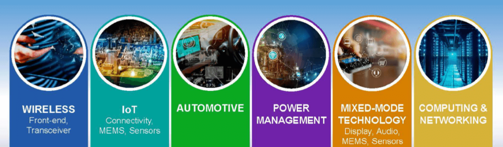
Figure 1 shows half a dozen distinct opportunities for semiconductors, and expresses a major change in our industry quite well: We no longer have one major application driving the progress of primarily digital SoCs — like mainframes, PCs, and smartphones have done in the past — but face a diverse spectrum of lower volume opportunities that often require a combination of heterogeneous functions. However, a few things have stayed the same: Customers always demand cheaper, faster, lower power, smarter and smaller electronic devices every 6 to 24 months. Are we now between a rock and a hard place and possibly doomed as individual companies or an entire semiconductor industry?
Not if we keep in mind “It is not the strongest of the species that survives, nor the most intelligent. It is the one that is most adaptable to change” and act accordingly. Some attribute this quote to Darwin, others to Magginson or Darrow. Anyway, based on my personal experience, I completely agree with whoever is the source of this quote.
Talking about change: What started as 3D IC technology – stacking dies vertically – has already been adapted by manufacturers to the diverse market requirements: Monolithic 3D NANDs, 3D ICs (like HBMs, HBM2s HMCs, image sensors), Interposer-based 2.5D ICs, multi-die FOWLPs and many of their derivatives. They are available as platforms or company-specific system-in-package (SiP) solutions to fit specific needs and offer system and IC designers a wide range of building blocks and integration alternatives to make (or keep) their designs competitive. High profile examples, in volume production, are AMD’s EPYC, Nvidia’s Volta and TSMC’s InFo technology. Many other companies, like Apple, Cisco, eSilicon, Global Foundries, Huawei, IBM, Marvell, NXP, Open-Silicon, Samsung, Xilinx, and others have demonstrated that choosing the right multi-die IC packaging technology and utilizing the modularity of their own or 3rd party packaging platforms – instead of following Moore’s Law – has become a key enabler for leapfrogging the competition.
Highlights from the 2017 3D ASIP Conference
This part 1 of my 3D ASIP blog focuses on general 3D IC topics and the keynotes presented at this conference. Part 2 will follow shortly and cover the in-depth presentations, delivered by focused experts, about many new and/or improved 3D IC related strengths.
General chair was Phil Garrou, technical co-chairs were Koyanagi-san from Tohoku University and CEA Leti’s Mark Scannell. The conference organizer was, like last year, IMAPS. The 14th 3D ASIP conference was held from Tuesday, December 5 to Thursday, December 7 in Burlingame, near the San Francisco airport.
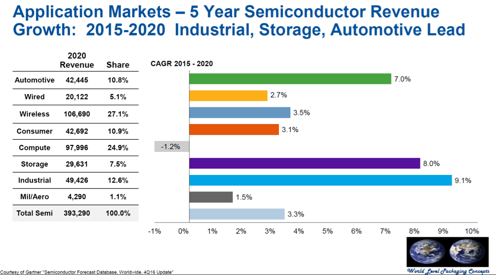
After three pre-conference tutorials on Tuesday morning, the first keynote speaker, right after lunch, was Jim Walker. He is well known from his many years at Gartner. Now he manages his own research company, WLP Concepts. Walker started by highlighting his projections for growth potentials of some of the very diverse, still somewhat overlapping, semiconductor markets ( Figure 2).
Walker predicted that the ongoing rapid consolidation of IC packaging vendors will continue, primarily because of the high capital investments needed to manufacture and test today’s advanced (often multi-die) IC packages. He also pointed out a few weak spots of our current silicon and packaging design and manufacturing EcoSystem:
- User-friendly design and verification tools and methodologies
- Fast and flexible fabrication processes
- More adaptable business environments for heterogeneous system integration.
The attending supply chain representatives agreed and expressed hope that the key beneficiaries of a strong ecosystem, the IC and system designers, would more aggressively demand these capabilities, of course at an attractive cost, and reward suppliers’ progress in these areas.
Wednesday morning started with another market research expert, Prismark’s Brandon Prior. In the second keynote, he presented how high-density interconnect solutions are migrating from concept to mainstream use. Prior covered both low-cost wafer-level packaging (WLP) as well as interposer-based high-end designs and made very compelling predictions for electronic systems and semiconductors utilizing these technologies.
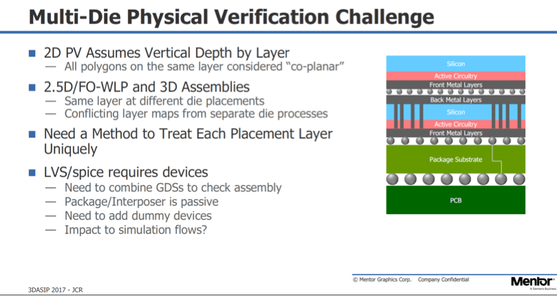
The third keynote of this conference was presented by Juan Rey from Mentor, a Siemens Business. He explained the import role Mentor’s die-package-board design tools and flows play, for quickly developing cost-effective high-density advanced packaging (HDAP) solutions. Rey emphasized that HDAP solutions require multi-physics verification steps for, e.g.: geometries and connectivity, electrical, thermal, mechanical and electromigration checks, to assure first-time success and IC reliability (Figure 8). He also mentioned that Mentor started multi-die focused development programs with AMD, Qualcomm, and TSMC already several years ago. Rey explained the focus of Mentor’s OSAT program and the ongoing Assembly Design Kit (ADK) development efforts with Amkor and ASE.
Right after lunch, the fourth keynote speaker, DARPA’s Dan Green took the stage to introduce the military’s perspective and DARPA’s many years of contributions to multi-die IC developments.`
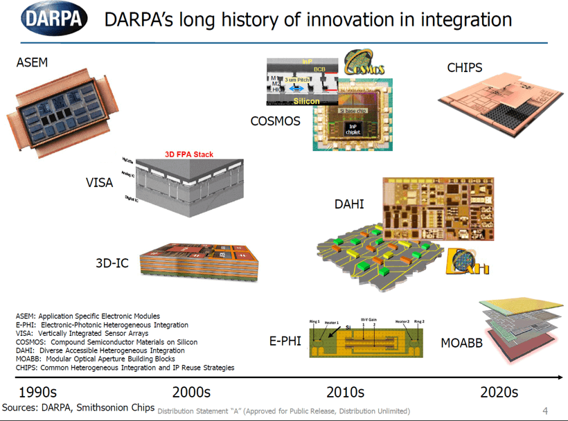
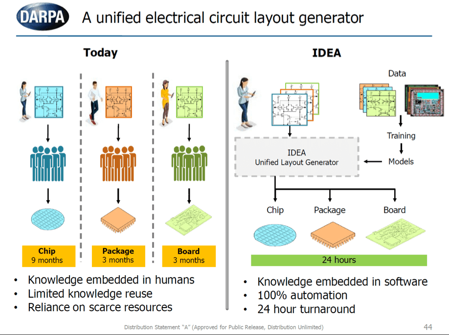
Green started out with a look back at DARPA’s long history in demanding and supporting integration efforts (Figure 3) and emphasized that the military needs density, heterogeneous integration and the benefits of modularity to develop and maintain electronic equipment for our military. In addition to contributing to manufacturing technologies, he stated that DARPA works with Cadence, Synopsys, and Keysight on EDA tools and flow, specifically for DARPA’s CHIPS program. DARPA needs methodologies to combine their custom chiplets (a.k.a. dielets) with off-the-shelf standard building blocks, to develop cost-effectively and (ideally) very quickly, electronic solutions. Green expressed that DARPA is very committed to contributing to the required ecosystem, including design flows, that will enable a rapid system scaling methodology.
The way I see it, the “100% Automation” statement in Figure 10 calls for EDA vendors to contribute now to chiplet development methods for designing and modeling. Also, EDA needs to contribute to an inter-connect method that facilitates combining chiplets on an interposer or package substrate. By engaging now on methodology developments, EDA vendors can create solid and useful starting points for fully automating – as soon as practical – well-defined and widely agreed upon design methodologies, not only for military applications.
Thursday morning started with the fifth keynote, addressing TSMC’s packaging technologies. Doug Yu positioned the InFO technology as lower cost, versus their very high-performance and high-bandwidth CoWoS technology, and InFO, as lower impedance versus flip-chip packages. He explained TSMC’s key criteria for every new IC packaging platform: performance, power, profile, cost, cycle time and scalability (P3 C2 S). Yu also talked about the tradeoffs between chip-first and chip-last flows and mentioned that their next-generation InFO packages will offer 1,5mm L/S and 1,5mm vias. He stated that TSMC starts about 100,000 wafers per month for InFO products and closed his presentation with a very important remark: “TSMC is no longer an IC foundry, we are now a system integration foundry!”
In addition to these five keynotes, 3D ASIP 2017 also offered more than 20 presentations from equipment and materials experts, actual users of 2.5/3D ICs academia and research centers. They described new advanced packaging capabilities and updated the audience on progress made with well-known activities, answered questions and engaged in 1-on-1 discussions during the breaks.
3D ASIP 2017 was the 10th edition of this conference I have attended. These ten conferences gave me enough data points for a quick look back in time and for a regression analysis to project the next few years.
First, a quick look back: The manufacturing ecosystem has made enormous progress in understanding and responding to the diverse technical market requirement, and has enabled the creation of reliable and much lower cost solutions. Most manufacturers have established constructive relationships between materials as well as manufacturing/metrology equipment vendors and their own assembly/test experts. A few years ago, all these manufacturers have selectively started to engage with EDA vendors – see a summary of Mentor’s presentation above – and have jointly worked with leading-edge IC and system designers to roll out high-performance computing/graphic/networking solutions, smart-watches, and other wearables.
Looking ahead, I would say: As I observed at IEDM 2017 very clearly, the previously ubiquitous solution of shrinking devices, according to Moore’s Law, to achieve cheaper, faster, smaller, smarter ICs is now much more selectively deployed and can no longer meet every market need.
As soon as the manufacturers, in cooperation with EDA vendors, develop many more library and IP building blocks (chiplets) and user-friendly die – package – board design methodologies for heterogeneous integration, the number of users will grow rapidly. Many medium and smaller companies will be able to join today’s relatively small group of multi-die IC designers, either as design services experts, chiplets developers or multi-die IC designers. Their many ideas, as well as markets and applications knowledge, will trigger a similar wave of technology adoption as I have seen in the 1980’s and ‘90’s for ASIC solutions.
Sorry, it’s beyond my pay grade to tell you exactly in which year the broad multi-die IC technology wave will be in full swing. ~ Herb