

The International Electronic Device Manufacturing Conference (IEDM) has always focused on device scaling, successfully guiding our industry for several decades along the challenging paths of Moore’s Law and the ITRS Roadmap. Both were primarily focused on digital functions. However, we all must agree that the real world around us is analog. To allow our electronic devices to better assist us in living comfortably in this analog world, we need to enable them to interact with all the analog signals around us. Because of this digital to analog shift in market requirements, the semiconductor industry stopped updating the ITRS roadmap in 2016 and formed a team of industry experts to focus on developing a Heterogeneous Integration Roadmap (HIR).
Integrating large amounts of logic, memory, analog, RF, MEMS, sensors, etc. on a single die has proven to not be economical. The increased market requirements for combining, in a very small form factor, heterogeneous functions, each one manufactured in the technically most suitable and very cost-effective process technology, has encouraged many IC packaging experts to develop manufacturing technologies for integrating multiple dies in single IC packages. The resulting multi-die ICs are not your father’s multi-chip modules (MCMs). They are much smaller, faster, lower power and above all, much lower cost solutions. They also enable large single-die SoCs to be partitioned into multiple homogeneous dies. This approach not only eliminates the transistor-count limit imposed by single-die SoCs, but also reduces silicon cost, non-recurring engineering (NRE), and development time. In addition, the resulting modularity offers flexibility, easier customization and significantly simplifies IP reuse in next-generation designs.
General Impressions
IEDM 2017 took place at San Francisco’s O’Farrell Hilton December 2-6, 2017. Kudos to the IEDM organizing team for reacting quickly to above-outlined changes in market requirements and including many multi-die topics in the 2017 IEDM agenda. All three keynotes on Monday morning focused on the benefits of looking beyond Moore’s Law. All seven presentations in the afternoon session #3 focused on how best to meet today’s market requirements by combining multiple heterogeneous or homogeneous dies and passive components in one IC package. These ten speakers offered system and IC design experts in attendance great opportunities to evaluate if, where, and how multi-die ICs can serve customer needs better than traditional single-die SoCs.
The IC Packaging-focused Keynotes
After a warm welcome by the General Chair, Stefan De Gendt, imec, Technical Program Chair, Ken Rim, Qualcomm, opened Monday’s Plenary Session.
The first keynoter, Lisa Su, AMD’s highly technical and business-savvy CEO, impressed the audience with her presentation, Multi-Chip Technologies to Unleash Computing Performance Gains over the Next Decade. AMD is one of the few 2.5D-IC pioneers in ongoing engagement with many supply chain partners to develop core capabilities for multi-die integration. AMD’s leading-edge 2.5D solutions clearly break down the dreaded “Memory Wall” and offer significant performance-per-Watt gains, compared to single-die SoCs. Su proudly demonstrated the benefits of adopting this IC design and manufacturing methodology for high-performance applications. She substantiated specific 2.5D benefits with Figures 1, 2 and 3 below. They clearly speak for themselves.
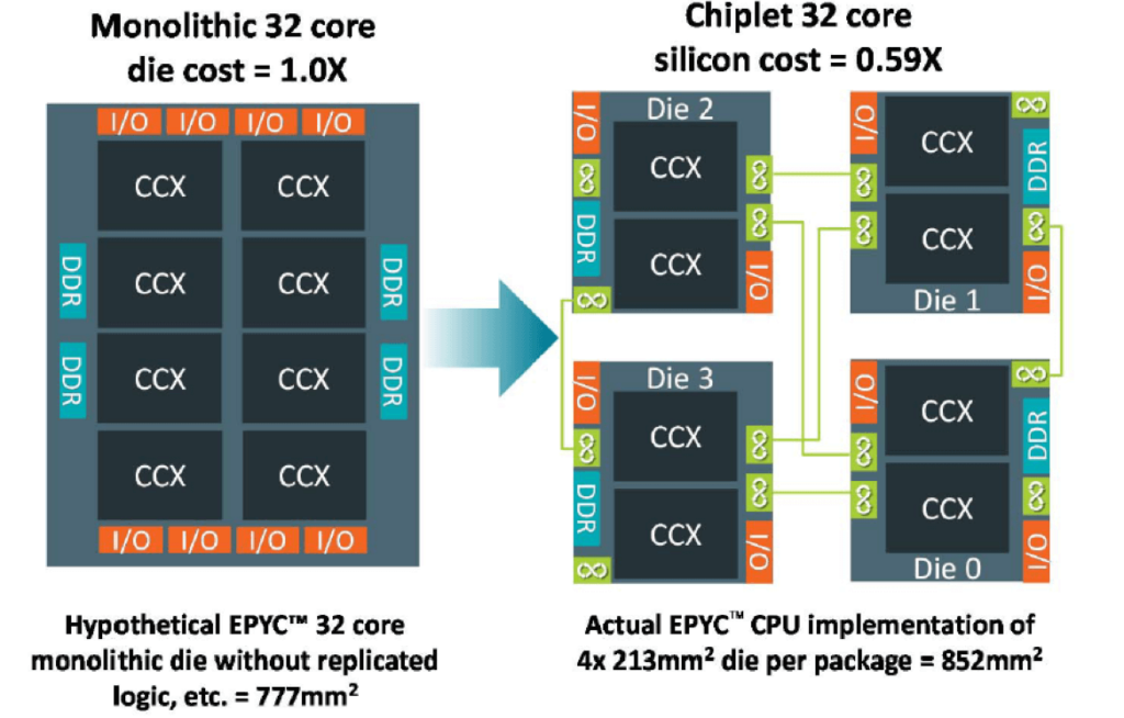
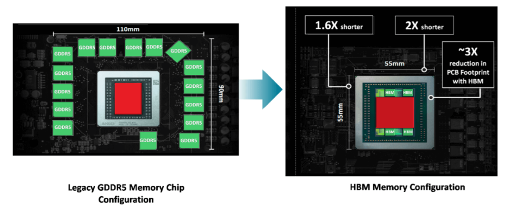
Beyond the silicon cost savings, shown in Figure 1, the multi-die EPYC CPU, combined with HBMs, also reduces the PCB area needed and its cost significantly. Figure 2 details the board space savings.
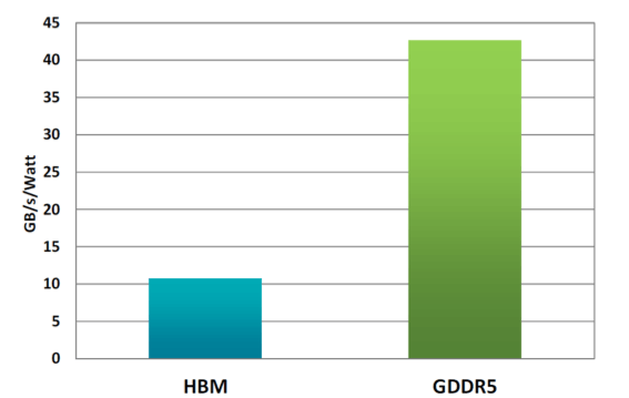
Performance-per-watt, the #1 criteria for success of a high-performance solution, benefits even more. Figure 3 shows that the energy-per-bit access with the previously used GDDR5 memory bank was 4x higher than in AMD’s new interposer design using HBMs.
In addition to these very telling figures, Su mentioned several other compelling reasons for no longer relying on the continued shrinking of device features and single-die SoC solutions:
- Wafer cost at 7nm is currently 4x higher than at 45nm
- The reticle limit of 500 – 600mm2 severely constrains design complexity
- The world is heterogeneous, therefore the digital processing unit may not remain the center of a system
The I/Os of a typical single-die SoC, designed to communicate with other ICs on a PCB, consume about 30% of the SoCs’ total power. This makes power management and cooling much more challenging, compared to interposer-based designs, which use very-low-drive I/Os with minimal electrostatic discharge (ESD) circuitry.
AMD’s modular and highly flexible multi-die architecture, developed in cooperation with leading-edge supply chain partners, positions AMD well for meeting current and future market requirements for highest performance-per-Watt compute engines.
In contrast to the first keynote that focused on system scaling from a silicon perspective, the third keynote, titled System Scaling for Intelligent Ubiquitous Computing, presented by TSMC’s Jack Sun, addressed the packaging challenges for system scaling. It demonstrated that the largest silicon wafer foundry is also fully committed to leadership in multi-die IC packaging. As an example of TSMC’s high-end leadership with its chip-on-wafer-on-substrate (CoWoS) technology, Sun described their very successful cooperation with Nvidia to develop the VOLTA GPU. This interposer-based GPU delivers 21 TFlops at only 300W power dissipation.
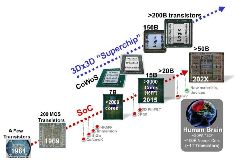
Sun’s presentation started by looking back to the first ICs comprising a few transistors and showed the industry’s progression towards >50 Billion transistor SoCs in the next few years (Figure 4). It also conveyed that TSMC’s so-called “3Dx3D Superchips” will soon exceed 200 Billion transistors. Sun explained that 3Dx3D refers to chips combining 3D transistors (a.k.a. FinFETs), 3D memories (e.g. HBMs) and 3D sensors. They can use TSMC’s CoWoS or InFO technology. He put this list of superlatives into context by pointing out that the human brain’s 3D structure has about 100 Billion neural cells, equivalent to 1 Trillion transistors, operating at only 20 Watts.
Nvidia’s Volta GPU is now the core of the highly successful Tesla V100 engine for machine learning. It is also deployed in Google’s Cloud Compute Engine. Beyond these highly visible successes, Sun talked about other designs benefitting from TSMC’s CoWoS technology, then showed the many InFO configurations TSMC offers today. Unlike I expected, he did not mention that TSMC captured all the A11 application processor business for iPhone X and 8.
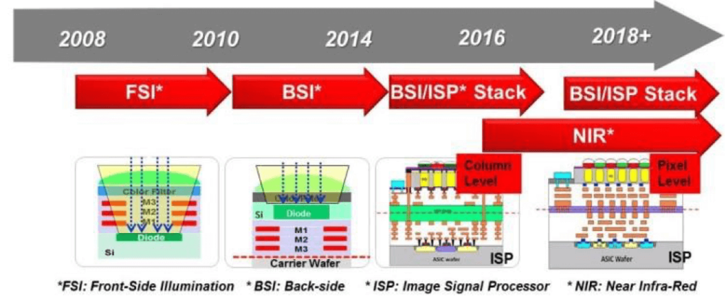
Another important application for multi-die die stacking, in this case vertically, are image sensors. TSMC also has a long and successful track-record in this segment. Figure 5 shows TSMC’s image sensor evolution.
A TSMC presentation would not be complete without mentioning its progress with and plans for CMOS logic and specialty technologies. Sun briefly described their work in multi-patterning and EUV and mentioned that they utilize directed self-assembly (DSA) to continue shrinking feature sizes. He explained that new materials are essential for manufacturing 5nm and possibly even smaller geometry ICs. TSMC expects that copper will still dominate as interconnect material and finds MRAM, RRAM and PCRAM to be promising memory technologies.
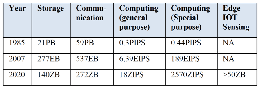
Unlike AMD’s Su and TSMC’s Sun, who both presented primarily available capabilities and demonstrated successes, the second keynote presenter, Adrian Ionescu, director of the Nanolab at EPFL in Lausanne, Switzerland, looked far into the future and covered a broad range of system-scaling topics. He substantiated his recommendations for actions with worrisome numbers. His presentation’s title, Energy Efficient Computing and Sensing in the Zettabyte Era: from Silicon to the Cloud, clearly conveyed the importance of very energy efficient designs for our industry’s growth. Ionescu showed a table to calibrate our expectations and direct our focus towards designing energy efficient ICs and systems (Figure 6). Considering that data centers in the U.S. consumed 2% of the country’s power in 2014 and an even higher percentage in 2017, the impact of the unchecked growth of data centers’ power consumption on our energy supply is very concerning.
Ionescu agreed with AMD’s Su and TSMC’s Sun that the benefits of following Moore’s Law are diminishing and eventually will end. According to Koomey, performance per Watt doubled every 1 ½ years until 2009, while it takes now almost 3 years to double. Ionescu also stated: In 5nm designs, 80% will be dark silicon. He explained in a very scientific way that to save energy, we’ll need to reduce supply voltages as low as SNR will allow, and/or operate transistors at much lower temperatures than we do today. Introducing steep slope switches, like tunnel-FETs, will also help improving performance per Watt.

Ionescu stated that 3D architectures can improve power efficiency by up to 1000x. Sounds great, however, he clarified that this factor applies only to monolithic 3D-ICs with fine-grain interconnects between the layers. Promising monolithic development efforts are ongoing at Leti. Ionescu also mentioned that a similar approach, driven by Philip Wong and Subashish Mitra, is ongoing at Stanford’s Nanoelectronics Lab.
Ionescu added, that Quantum computing and neuromorphic computing are also methodologies to improve computing efficiency. He emphasized too, that the architecture of an IoT network significantly impacts the power it consumes for computing and communications.
Focus of IEDM’s Session 3: IC Packaging
Out of the many parallel sessions, IEDM offered, I chose the IC packaging-focused presentations. Seven well-known industry experts updated the audience on the progress of their development efforts.
Leti’s Pierre Batude, representing a large CEA Leti and STMicroelectronics R&D team, talked about 3D Sequential Integration: Application-Driven Technological Achievements and Guidelines. He outlined their progress and plans for CoolCubeTM, a development effort towards enabling 3D logic as well as integrating heterogeneous functions monolithically.
For Sony, the clear market leader in image sensors, Hidenobu Tsugawa presented Pixel/DRAM/Logic 3-layer Stacked CMOS Image Sensor Technology. He described characteristics and benefits of their current designs, using Invensas’ DBI® technology, and outlined development goals for the ongoing cooperation with AMAT and Coventor.
Cian O Mathuna from the University of Cork, Ireland, talked about Power Inside – Applications and Technologies for Integrated Power in Microelectronics. He described a highly efficient (91.7% at 0.5W) on-chip PMIC, using thin-film and magnetic-core inductor technology.
GeorgiaTech’s Rao Tummala covered 3D System Package Architecture as Alternative to 3D Stacking of ICs with TSV at System Level, and listed achievements of his 3D Systems Packaging Research Center and how they cooperate with industry leaders to develop a wide range of multi-die IC packaging solutions.
Luke England, from Global Foundries, described how Advanced Packaging Saves the Day! – How TSV Technology Will Enable Continued Scaling. He outlined how Global Foundries, in cooperation with major assembly houses (OSATs), serves customer requirements with 2.5D and 3D-ICs.
TSMC’s Douglas Yu talked about “Advanced Packaging with Greater Simplicity” and complemented TSMC’s morning’s keynote with many more details about TSMC’s backend services and their broad IC packaging offering. Yu also explained why TSMC sees the performance, power, profile, cost, cycle time and scalability (PPPCCS) criteria of a packaging platform as essential for their success in IC packaging.
Last, but certainly not least, IBM Zurich’s Thomas Brunschwiler, explained in his presentation Towards Cube-Sized Compute Nodes: Advanced Packaging Concepts enabling Extreme 3D Integration what his team is working on to enable very higher performance computing from a packaging perspective. He described how they cool a 622-Watt supercomputer, the size of a sugar cube, by pumping a liquid through channels in interposers.
Thanks for reading my blog about the IEDM presentations I attended on Monday, Dec 2. Sorry, I couldn’t attend IEDM for the rest of the week, because of the entirely IC packaging-focused IMAPS’ 3D ASIP conference, held from Tuesday to Thursday near SFO, required my attendance. More about this conference shortly. ~ Herb


