
The foundry world has been big news in the past few weeks. TSMC started up the Kumamoto Fab, Japan’s leading-edge semiconductor technology center, partnering with Tenstorrent on RISC-V and chiplets to be manufactured at Rapidus. The biggest non-surprise news flash was the roll-out of Intel’s Foundry Direct Connect, which they touted as the first systems foundry for the AI era.
While Intel has been discussing the foundry business for some time, the get-together laid out some additional plans for Intel’s foundry effort. Intel has a full array of IP and EDA vendors; Siemens, Synopsis, Cadence, Ansys, Keysight, and Lorentz Solutions. There is also a collaborative effort with ARM to provide leading-edge services for ARM SoC designs. This effort appears to be focused on startups developing technology with ARM-based technology. RISC-V technology has also been mentioned in the design mix.
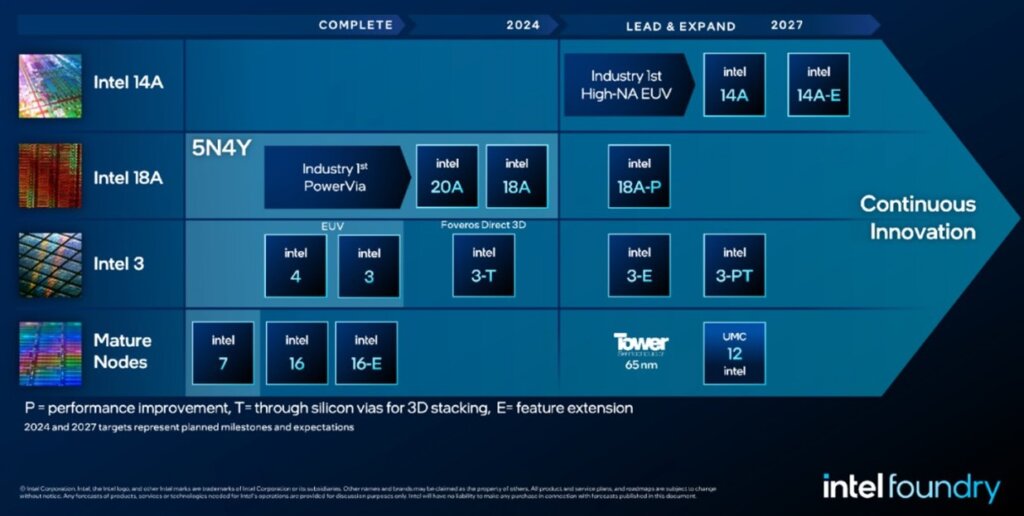
This is significantly different from the first Intel Foundry effort where X-86 and ARM were the core technologies used for design. Intel laid out its technology roadmap, which includes the partnerships with Tower Semiconductor and UMC thus adding some foundry experience to their effort.
What the Pundits Say about Intel Foundry
Intel’s previous foundry efforts floundered. Early customers included Altera and Achronix Semiconductor Corp. to manufacture its FPGAs. Cisco and Panasonic also came on board. However, delays in chip designs, and in reviewing several articles on the topic, a lack of focus on the customer were some of the causes for failure. Daniel Nenni, of SemiWiki, in December of 2017 wrote. “Great intentions, good effort, too many broken promises, but doomed from the very beginning, my opinion.”
There are many mixed opinions on the future success of the New Intel Foundry. Darren Grasby of AMD and Dr. Yang Guang-Lei who has worked at both TSMC and Intel are both skeptical of Intel Foundries’ future success. Dr. Yang cites a lack of customer-centric engineering at Intel. And Grasby says he thinks the new path is the wrong one. Pat Gelsinger, CEO of Intel, currently gives the project a passing grade.
However, in this foundry go-round, there are differences. The first is the reorganization of the company. Intel’s vaunted manufacturing group has been separated into a stand-alone business. This means for the first time the manufacturing team will have profit and loss to contend with.
Will this make the manufacturing team more efficient and competitive? What will happen to the copy exact policy? What changes will take place to improve operating expenses? Only time will tell! The fact that the Intel chip design teams can choose where they want to manufacture their products, either at Intel or a competing factory will require the manufacturing team to become more efficient and competitive to retain the internal business. Intel is already manufacturing some products at TSMC, which makes the transition even more interesting. Nvidia is also hinting that it may use Intel for some of their production.

A second difference is the appointment of a foundry advisory committee to help guide Intel in the foundry business. One of the key focuses of this committee is to help drive a continuous customer-first culture across the Intel Foundry organization. Intel has listened to some of the criticism of their first foundry effort.
A critical part of the Intel Foundry effort focuses on building AI chips. In part, this means heterogeneous integration or 3D packaging. One of the challenges the AI industry has faced is a packaging capacity shortage. TSMC has been ramping up its 2.5/3D packaging capacity to help meet demand, but if you listen to Nvidia, there are still constraints in the manufacturing of Nvidia’s AI system. With Intel opening the doors to its EMIB and Foveros packaging technology, companies now have an alternative to TSMC’s advanced packaging capability. There does seem to be one catch. With the lack of industry standards, there is a high probability if a company is looking for an advanced 3D chiplet package, they will also need to have their chips manufactured by either TSMC or Intel and then packaged by TSMC or Intel. The exception will be the DRAM chips, where the interface will need to match that of the packaging technique. One other point is that with access to the Intel packaging foundry, chips will not have to travel overseas for the packaging part of the process.
The 20+ billion-dollar question, is will the new Intel foundry model be successful? The company has a list of interested customers, but they did last time as well. The eco-system looks to be better, and it appears to have a better support structure than the previous effort, and they appear to have addressed some of the criticism from the previous efforts.
The keys will be, can the manufacturing and design teams deliver what the customer wants in a timely manner, and will the pricing be competitive, or have a time-to-market advantage over the customer’s current models. To achieve Intel’s lofty goals the effort will need to improve from a passing grade to at least second in the class. Only time will tell if Intel will be successful this time around.


