
Automotive compute processors are rapidly adopting advanced process nodes. NXP announced the development of 5nm automotive processors in 2020 [1], Mobileye announced EyeQ Ultra using 5nm technology during CES 2022 [2], and TSMC announced its “Auto Early” 3nm processes in 2023 [3]. In the past, the automotive industry was slow to adopt the latest semiconductor technologies due to reliability concerns and lack of a compelling need. Not anymore.
The use of advanced processes necessitates the use of advanced packaging as seen in high-performance computing (HPC) and mobile applications because [4][5]:
- While transistor density has skyrocketed, I/O density has not increased proportionally and is holding back chip size reductions.
- Processors have heterogeneous, specialized blocks to support today’s workloads.
- Maximum chip sizes are limited by the slowdown of transistor scaling, photo reticle limits, and lower yields.
- Cost-per-transistor improvements have slowed down with advanced nodes.
- Off-package dynamic random-access memory (DRAM) throttles memory bandwidth.
These have been drivers for the use of advanced packages like fan-out in mobile and 2.5D/3D in HPC. In addition, these drivers are slowly but surely showing up in automotive compute units in a variety of automotive architectures as well (Figure 1).
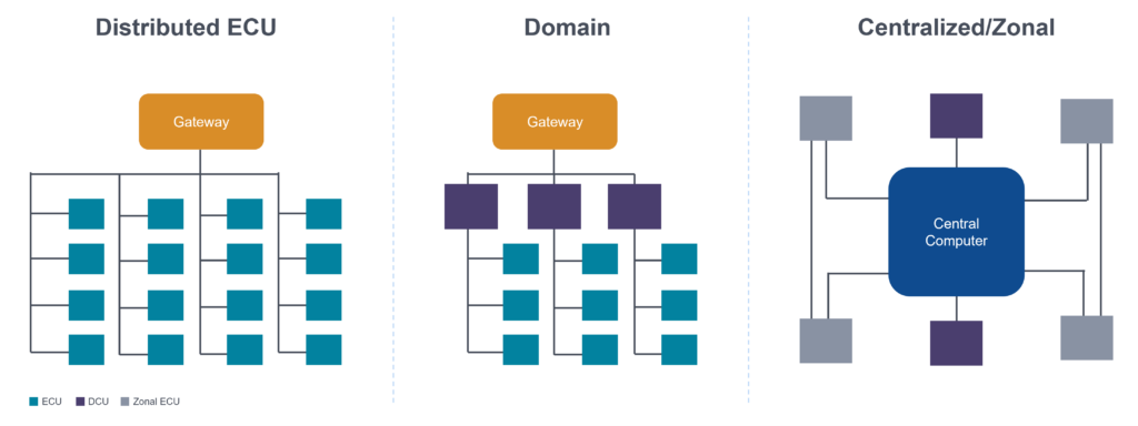
Vehicle electrical/electronic (E/E) architectures have evolved from 100+ distributed electronic control units (ECUs) to 10+ domain control units (DCUs) [6]. The most recent architecture introduces zonal or zone ECUs that are clustered in physical locations in cars and connect to powerful central computing units for processing. These newer architectures improve the scalability, cost, and reliability of software-defined vehicles (SDVs) [7]. The processors in each of these architectures are more complex than those in the previous generation.
Multiple cameras, radar, lidar, ultrasonic sensors, and more feed data into the compute units. Processing and inferencing this data require specialized functional blocks on the processor. For example, the Tesla Full Self-Driving (FSD) HW 3.0 system-on-chip (SoC) has central processing units (CPUs), graphic processing units (GPUs), neural network processing units, Low-Power Double Data Rate 4 (LPDDR4) controllers and other functional blocks – all integrated on a single piece of silicon [8]. Similarly, Mobileye EyeQ6 has functional blocks of CPU clusters, accelerator clusters, GPUs, and an LPDDR5 interface [9].
As more functional blocks are introduced, the chip size and complexity will continue to increase. Instead of a single, monolithic silicon chip, a chiplet approach with separate functional blocks allows intellectual property (IP) reuse along with optimal process nodes for each functional block [10]. Additionally, large, monolithic pieces of silicon built on advanced processes tend to have yield challenges which can also be overcome using chiplets.
Current advanced driver-assistance systems (ADAS) applications require a DRAM bandwidth of less than 60GB/s which can be supported with standard double data rate (DDR) and LPDDR solutions. However, ADAS Level 4 and Level 5 will need up to 1024 GB/s memory bandwidth which will require the use of solutions such as Graphic DDR (GDDR) or High Bandwidth Memory (HBM) [11][12].
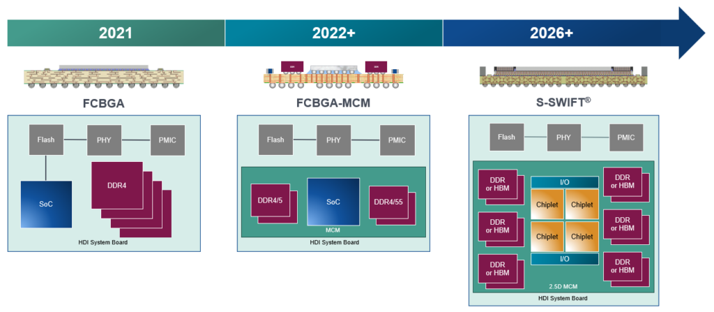
Automotive processors have been using flip-chip ball grid array (FCBGA) packages since 2010. FCBGA has become the mainstay of several automotive SoCs such as EyeQ from Mobileye, Tesla FSD, and NVIDIA Drive. Consumer applications of FCBGA packaging started around 1995 [13], so it took more than 15 years for this package to be adopted by the automotive industry. Computing units in the form of multichip modules (MCMs) or system-in-package (SiP) have also been in automotive use since the early 2010s for infotainment processors. The use of MCMs is likely to increase in automotive computing to enable components like the SoC, DRAM, and power management integrated circuits (PMIC) to communicate with each other without sending signals off-package.
As cars move to a central computing architecture, the SoCs will become more complex and run into size and cost challenges. Splitting these SoCs into chiplets becomes a logical solution and packaging these chiplets using fan-out or 2.5D packages becomes necessary. Just as FCBGA and MCMs transitioned into automotive from non-automotive applications, so will fan-out and 2.5D packaging for automotive compute processors (Figure 2). The automotive industry is cautious but the abovementioned architecture changes are pushing faster adoption of advanced packages. Materials, processes, and factory controls are key considerations for the successful qualification of these packages in automotive compute applications.
In summary, the automotive industry is adopting advanced semiconductor technologies, such as 5 nm and 3 nm processes, which require the use of advanced packaging due to limitations in I/O density, chip size reductions, and memory bandwidth. Processors in the latest vehicle E/E architectures are more complex and require specialized functional blocks to process data from multiple sensors. As cars move to the central computing architecture, the SoCs will become more complex and run into size and cost challenges. Splitting these SoCs into chiplets becomes a logical solution and packaging these chiplets using fan-out or 2.5D technology becomes necessary.
Editor’s note: This article first appeared in the 2024 3D InCites Yearbook. Read the full issue here.
References
[1] NXP. “NXP Selects TSMC 5nm Process for Next-Generation High-Performance Automotive Platform.” NXP.
[2] Mobileye. “Mobileye at CES 2022.” Mobileye.

[3] Business Wire. “TSMC Showcases New Technology Developments at 2023 Technology Symposium.” Business Wire.
[4] Swaminathan, Raja. “Advanced Packaging: Enabling Moore’s Law’s Next Frontier Through Heterogeneous Integration.” HotChips33.
[5] SemiAnalysis. “Advanced Packaging Part 1” SemiAnalysis.
[6] McKinsey & Company. “Getting Ready for Next-Generation EE Architecture with Zonal Compute.” McKinsey & Company.
[7] NXP. “How Zonal E/E Architectures with Ethernet are Enabling Software-Defined Vehicles.” NXP.
[8] WikiChip. “Tesla (Car Company)/FSD Chip.” WikiChip.
[9] Mobileye. “EyeQ Chip.” Mobileye,.
[10] Ziadeh, Bassam. “Driving Adoption of Advanced IC Packaging in Automotive Applications.” Presentation at IMAPS DPC, March 2023. General Motors, Fountain Hills AZ, March 16, 2023.
[11] K Matthias Jung and Norbert Wehn. “Driving Against the Memory Wall: The Role of Memory for Autonomous Driving.” Fraunhofer IESE, Kaiserslautern, Germany, and Microelectronic Systems Design Research Group, University of Kaiserslautern, Kaiserslautern, Germany. Kluedo.
[12] Micron. “Cinco de Play: Memory – Is That Critical to Autonomous Driving?” Micron.
[13] McKinsey & Company. “Advanced Chip Packaging: How Manufacturers Can Play to Win.” McKinsey & Company.