
NIST held the “Chiplet Interfaces Technical Standards Workshop” at the NIST National Cybersecurity Center of Excellence in December 2023.
During this workshop, technical experts from industry, academia, standards-setting organizations, and industry alliances gathered to discuss and prioritize specific standards efforts related to chiplet-based architectures with a focus on physical and logical interfaces, aiming to drive progress in the semiconductor and microelectronics industry.
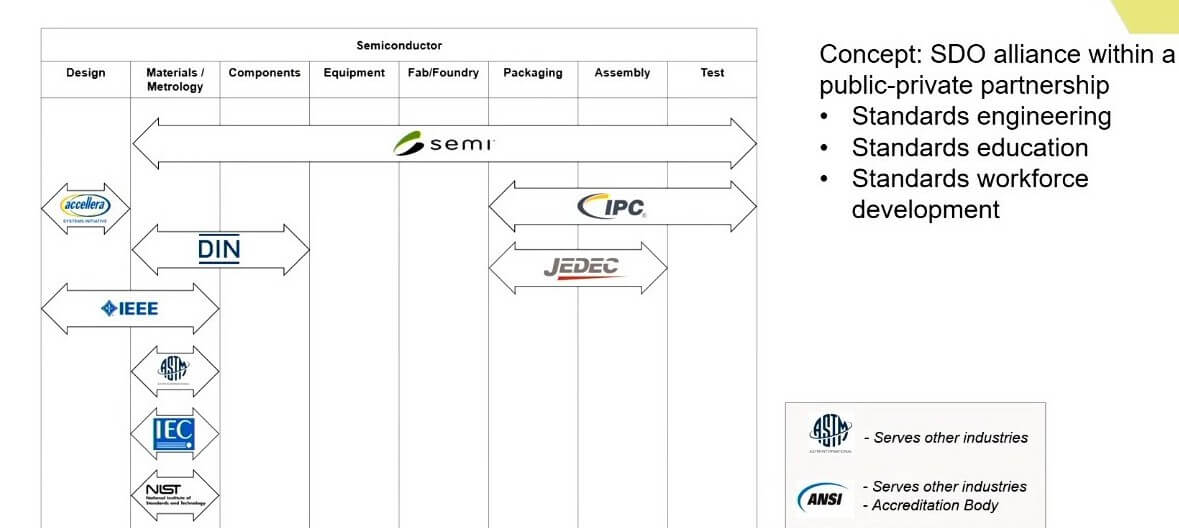
Let’s first take a look at what areas the typical standards groups are working in.

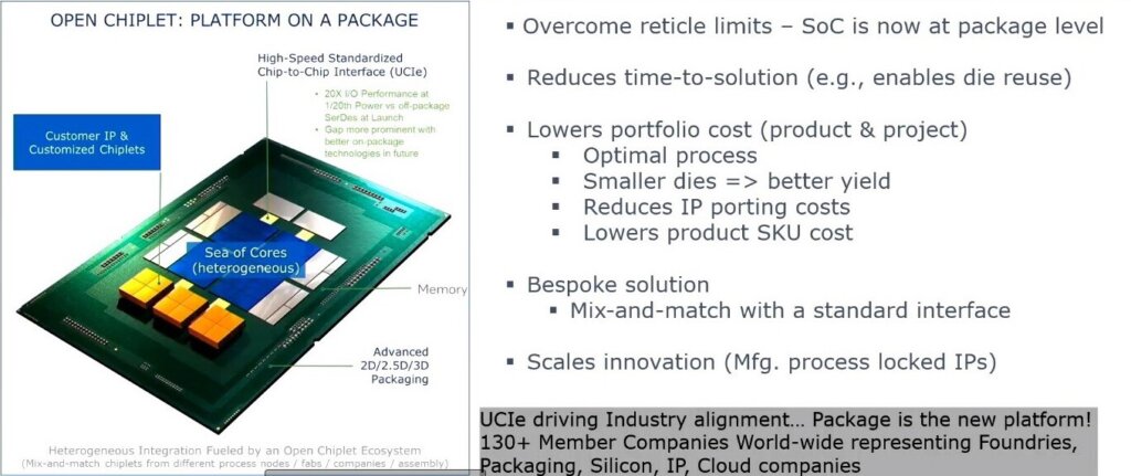
Debendra Das Sharma, Intel Sr Fellow and co-inventor and chairman of the UCIe chiplet interconnect standard shared his input on what is now the leading chiplet industry standard.
In Sept of 2023, Intel revealed the test chip “Pike Creek” containing an Intel UCIe chiplet fabricated on IFS Intel 3, a Synopsys UCIe IP chiplet fabricated using the TSMC N3E process node and packaged using Intel EMIB technology.
This successful pairing mimics the mixing and matching of dies that can occur in real-world multi-die chiplet modules, demonstrating that this approach is commercially viable. Intel’s plans to transition from proprietary interfaces to the UCIe interface in its next-generation Arrow Lake consumer processors further underscore the importance of this breakthrough (Figure 2).
UCIE supports both standard and advanced packages as shown in Figure 3.
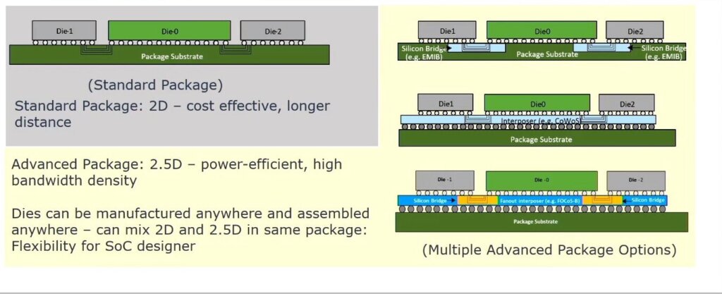
Figure 3: UCIe 1.0/1.1 supports standard and advanced packages.

Dr. Sreejit Chakravarty whose career includes positions at Intel, LSI, and Avago currently chairs the IEEE P3405 work group on Chiplet Interconnect Test and Repair, which aims to standardize the test and repair of chiplet interconnects.
This standard defines effective and efficient mechanisms to test and repair chiplet interconnects. The standard includes the following:

- An Architecture definition for the test and repair of chiplet interconnects. The architecture consists of the following elements: chiplet interconnect clustering, cluster clocking and redundancy, cluster repair muxing and mux re-configuration support, lane numbering, and repair signature format. In addition, the standard defines testing support for high-volume manufacturing of chiplet interconnects.
- A description language that defines the test and repair hardware, the signature format, the message format for communication between the two dies and the die models used for validating the test infrastructure.
Table 1: Feature, feature trend, and test implications for chiplet interface standards.
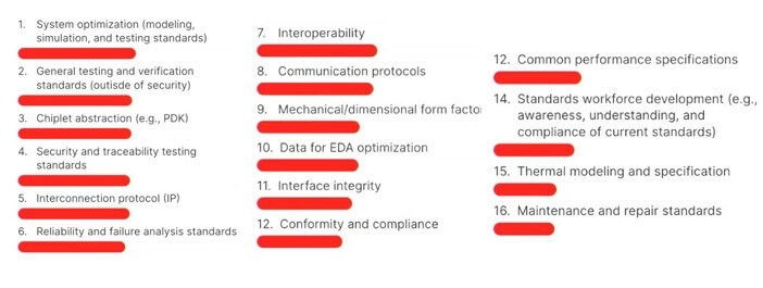
Most of Day 2 was taken up by attendees prioritizing what standards need to be worked on. The final prioritization list, decided by attendees, is shown in Figure 4.
Samsung To Set Up Chip Packaging Research facility in Japan
Samsung announced that it will invest around $280MM over five years in building a facility for advanced chip packaging research in Japan’s Kanagawa prefecture near Yokohama.
Japan reportedly will provide Samsung subsidies worth up to 20 billion yen as it looks to support the revitalization of domestic chip manufacturing. Samsung reportedly already has a research and development center nearby and felt this move would deepen ties with Japanese equipment and materials suppliers.
For all of the latest on Advanced Packaging stay linked to IFTLE…………………….


