
I was first exposed to chiplet technology in 2017 when Lisa Su presented the concept at the IEEE IEDM meeting. At that time, I thought it made sense, as the industry had been doing systems-in-package (SiP) for several years and chiplets seemed very much the next step in advanced computing. The industry faced challenges, such as the need for parallel processing in big data, and the emerging AI space. So the ability to add processors to the package was one way to address the training and data-crunching requirements.
Fast forward 5 years to January of 2023 to the first annual Chiplet Summit, held January 24-26, 2023. The conference was organized and run by Semper Technologies. Semper Technologies will be holding the second annual Chiplet Summit in January 2024.
The organizers report registration of 520 with 320 in attendance, and 40 exhibitors. By my count the conference room was set up for 200 and the room was about half full. The format was a day of tutorials, followed by two days of keynotes in the morning, and panel sessions in the afternoon, with four parallel tracks. With a two-hour lunch each day and a reception on Wednesday evening there was plenty of time for networking.
Since I’ve been exposed to the heterogenous integration market for a few years and spent a bit of time as an analyst in a previous life, I was looking for “the, what is new in chiplets” at the conference. A significant number of the keynotes focused on their perspective of the why in chiplets. What follows is my interpretation of the shortlist.
Discussions ranged from how large die suffers from yield issues, reticle limitations, the ability to generate significant compute power, and better reuse of IP, the memory wall; to AI training, inferencing, latency, heat issues, design, and integration of different die/chiplets together. For someone with years of experience in heterogeneous integration, this might have been a bit too much of a review. However, many audience members were just learning about chiplets, so the different perspectives of the talks gave them a good education regarding the industry.
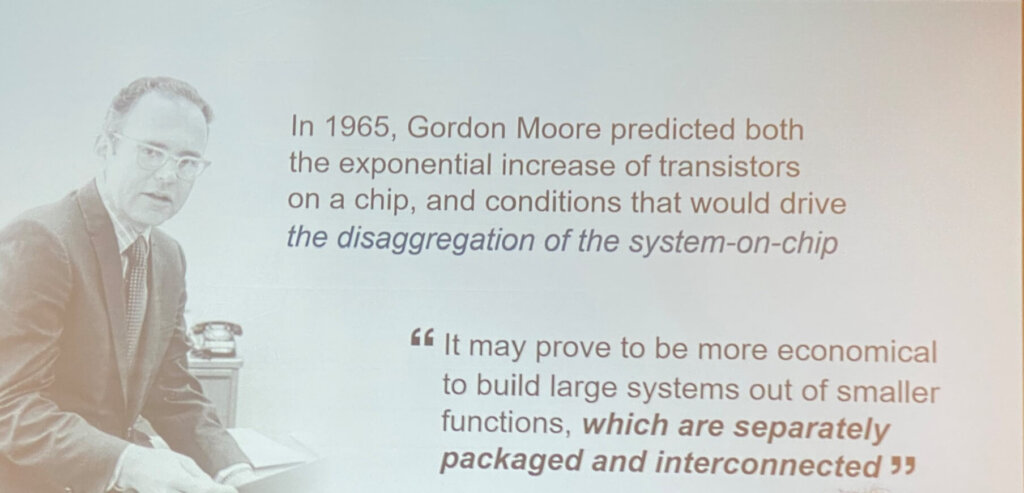
Having spent a lot of time writing and discussing Moore’s law in the past, including making comments about Moore’s law in the third dimension, I was surprised to find out that in his paper, Moore had allowed for the fact that it might prove to be more economical to build large systems out of smaller functions, which are separately packaged and interconnected. As chiplet packaging moves into the third dimension, it appears this, and the new 3D SiPs being marketed, still fall under Moore’s law (Figure 1).
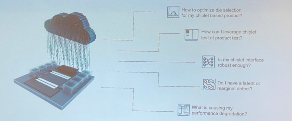
Of all the presentations, one, in particular, stood out for me. Nitza Basoco, VP of Business Development at protean Tecs, discussed agent-based monitoring. Her thesis is that we will solve the technical, but Murphy’s Law will prevail. Having spent a great deal of time in manufacturing I’m a firm believer in Murphy. Basoco described that in building chiplets you need to make tradeoffs. However, those tradeoffs can prove to be problematic, and finding complex issues can be challenging. As one can imagine, a heterogeneously integrated package is difficult to test, but testing will be a critical part of the process. Basoco proposed that by using agent-based monitoring, perhaps we can gain a better understanding of chiplet reliability and determine which parts are problematic, fix those areas, and optimize chiplets (Figure 2).
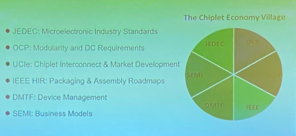
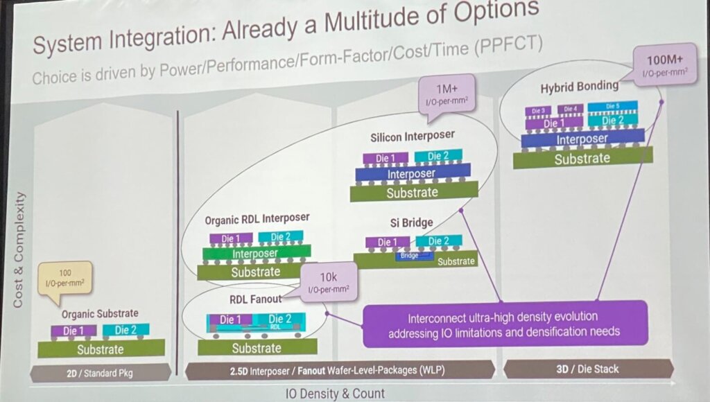
With chiplets being a new entity, the standards are still being developed. There were several presentations on standards committees. Bapi Vinnakota with the open compute (OCP) foundation laid out that it will take a village to develop the standards needed as chiplets and heterogenous integration continue to evolve (Figure 3). However, during the conference, it was also argued that multiple standards may emerge, especially as Intel, TSMC, and Samsung each have successful chiplet packaging products in production, and there are OSATS with chiplet capability.
At the conference, I moderated a panel on the future of chiplets. The panelists were Erez Shaizaf, CTO, Alchip; Robert Patti, President, nHanced Semiconductors; Craig Bishop, CTO, Deca; Mike Li, VP of Engineering/New Products, Corigin

The Wednesday panel discussions summarized the conference well. Chiplets, in the form of SiPs, have been around for a considerable time. The panel mentioned that 2.5 and 3D technologies had been accessible for nearly 20 years. And two of the panelists had been working on the technology since the mid-2000s. The industry will continue to develop manufacturing methods to reduce the impact of getting rid of the heat, the best way to wire, or get rid of the wire, and what type of interposer, silicon, glass, organic, or possibly none. The panel referenced the industry transition from printed circuit boards to heterogenous integration using chiplets.
There was an interesting discussion surrounding intellectual property. One panelist suggested that the IP vendors would need to re-visit their business models as IP would only be sold once, and there was one thought that the IP might become more complex. There was agreement that heterogeneous integration IP needed to catch up with the market.
The standards discussion stressed that standards are good, but it is likely that there will be multiple standards, possibly centered on the current large manufacturers producing chiplets. So, you would have the Intel standard, the TSMC standard, the Samsung standard, and potentially the OSAT standard. It was also mentioned that standards impacting chip design and IOs are likely to be for advanced chips, processors, GPUs, and memory. The panel thought that legacy chips 14nm and above would probably not change to adapt standards, due to the costs that would be involved in a redesign and tape out. This would require chiplet integrators to be flexible with their designs (Figure 4).
The panelists agreed that as chiplet technology gains momentum there is the potential for lots of new fabless chip or chiplet manufacturers. The thinking was that heterogeneous integration enables a new level of creativity that can be implemented at an economical level, as you are no longer needed to design and tape out an SoC. You can buy off-the-shelf chips and make your own application-specific product in a package. When I heard that I smiled. A co-worker of mine was proposing that over 20 years ago.


