More on Reshoring Microelectronics
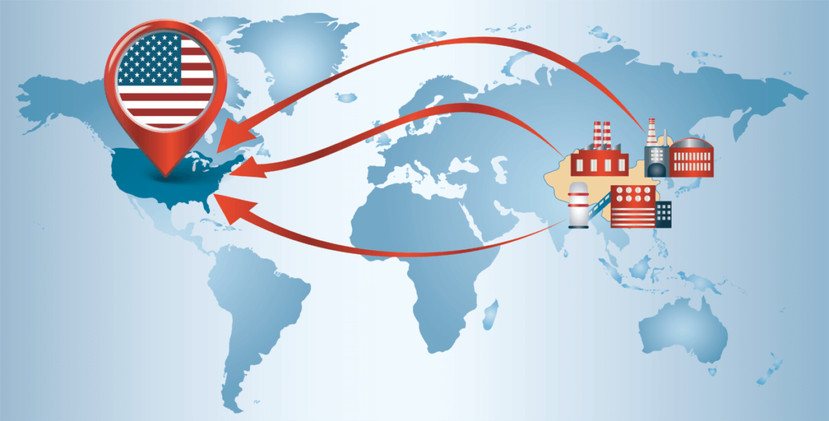
By now everyone is aware that the US government, triggered by the pandemic, is in the process of attempting to bring parts of the electronics industry that left our shores (mainly for cheaper Asian production), back onshore. [ see IFTLE 463: DoD Focused on Reshoring Electronics to the US]
Federal Computer Week just did an interesting piece Congress Moves to Bring Back Domestic Microelectronics Manufacturing”, and I’d like to highlight their point on printed circuit boards (PCBs).
Due to growing competition with China and national security concerns heightened by the pandemic, the Congress and the Department of Defense (DoD) have pushed to tighten its cybersecurity and technical supply chains. According to FCW, The Defense Department will have to stop using PCBs made in China, Russia, North Korea, and Iran, and other potentially adversarial countries in its mission systems starting in 2023, according to a provision in the 2021 defense policy bill. Last time I checked my desktop was free of Iranian PCBs. but not so with Chinese parts.
While regulations on PCB manufacturing won’t come out until mid-2022, changes are expected to occur in the next year as the DOD works with electronics companies, contractors, and suppliers to determine sourcing and capability needs. In addition to the new sourcing requirements, Congress also requires DOD to study the effects of expanding the restrictions to include commercial PCBs and assemblies.
AIM Photonics

Let’s take a look at some of the information Ed White, Assoc. VP recently shared on an AIM Photonics webcast broadcast by Semiconductor Digest.
The organization, located in Rochester NY, came into being in 2015 as one of the DoD National Manufacturing Innovation institutes under the MANTECH program. Since then, the company has gone through several expansions. It is currently predominantly a 300mm facility and is expanding its presence in test, assembly, and packaging to augment its capabilities in photonics.
AIM reportedly has 12K sq ft of class 1000 cleanroom. It is an open-access facility being run like an institute, not a university research lab. By that I mean they build the prototypes for you and then help transfer the process to a standard commercial operation if scaleup is required.
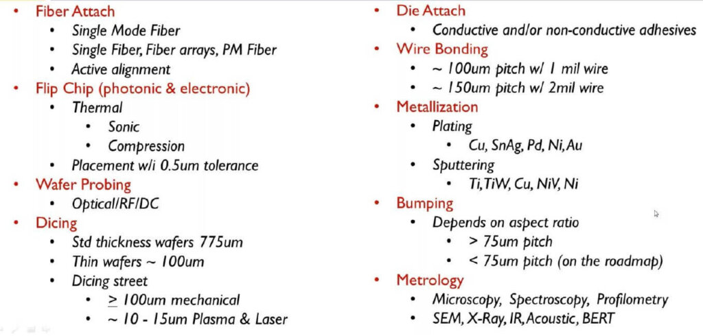
Its tool capabilities are extensive and are shown below:
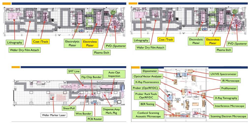

And of course, AIM’s photonics facility.
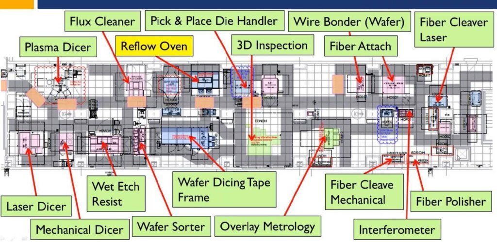
Capabilities include:
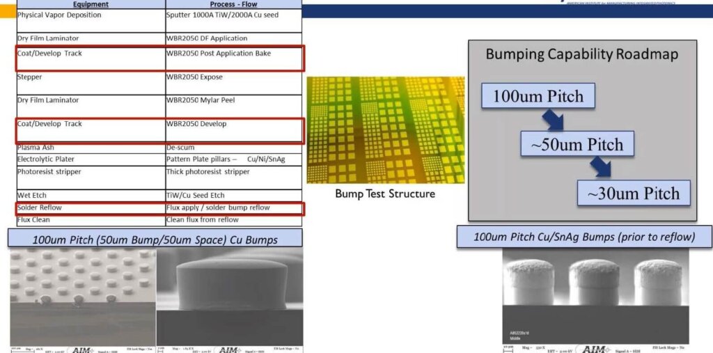
Ed described a developing bumping technology with AIM’s first bumping customer already engaged in a program with them. They currently profess capability down to 75um with 55 and 36µm on its future roadmap.
He also sees an opportunity for developing RDL capability and is currently in the planning stages for that.
They certainly are one of the most advanced institutes in the US for photonics module development including fiber and laser attach.
For all the latest in Advanced Packaging stay linked to IFTLE…………………………