
My, it has been a busy month for virtual conferences in the microelectronics space. During the week of October 5th, there were four virtual conferences I had an interest in that were running simultaneously. Having a day job that limits my computer time during the day, I had to be selective, and needless to say, I am still digging out, or in this case, Zooming out. The good news and bad news of virtual conferences are that organizations are taking advantage of the platform to keep folks engaged, and the formats are continuing to improve. The bad news is that multiple conferences are all in the same time frame, and presenters still need to make sure their virtual set up is conducive to a professional presentation. I am sure there are some Marcom/AR folks out there that cringe when they go back and review these talks. One last gripe and then I’ll move on is that it always seems that one of the keynotes that I really want to see is not available at a later date when I finally have time to sit down and watch the conference. I’m hoping this changes in the future, while we continue to be in a virtual world.
The conferences I was able to fit into my schedule were ARM’s Developer Summit and the 2020 IITC. I missed the MEM’s congress and the Nvidia GTC conference. All of the conferences have relevance to the 3D packaging market.
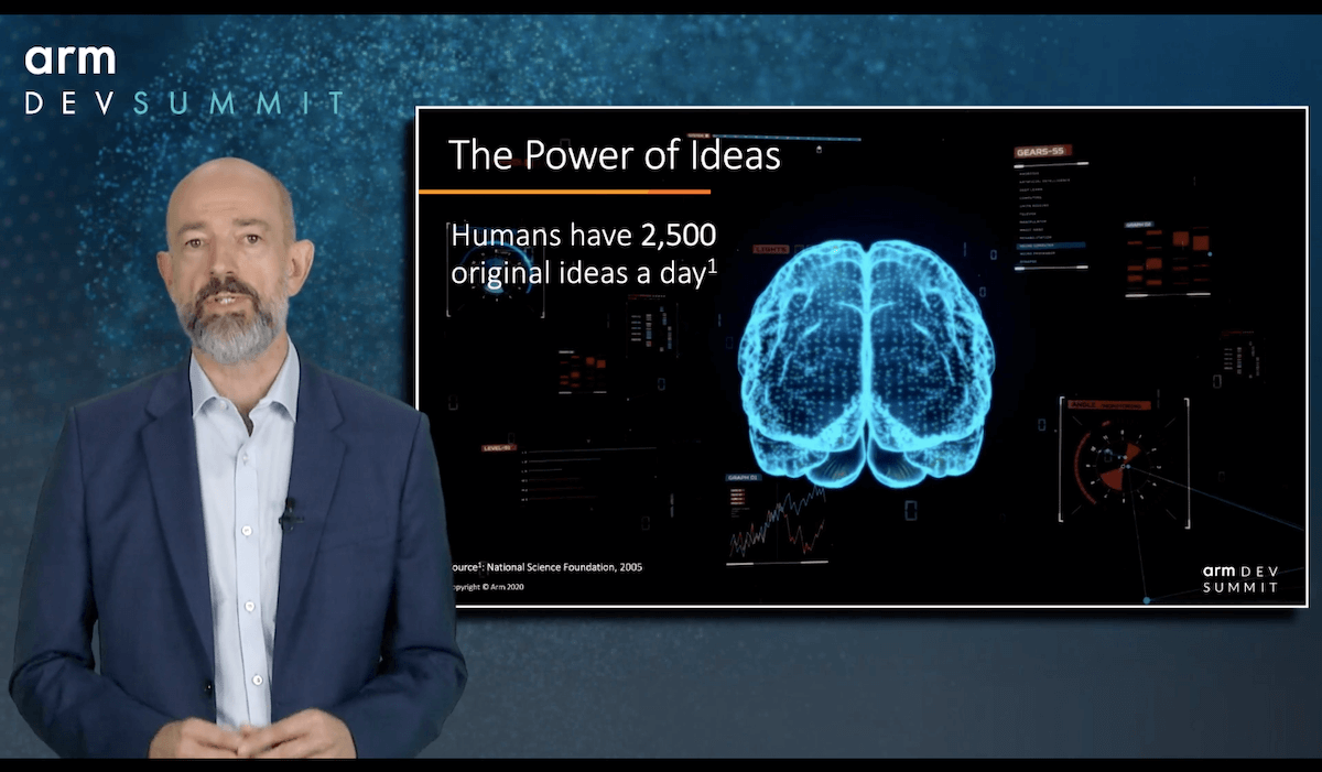
ARM Developer Summit
The ARM developer conference always gives a good peek at what is happening in the non-X86 compute world. In the past this meant Microcontrollers (MCUs) and field-programmable gate arrays (FPGAs); however, in the era of artificial intelligence and machine learning (AI/ML) processing, which Jem Davis states is “once in a lifetime occurrence”, a one-size-fits-all compute platform may not be as effective as the ability to design specific hardware than software that fits a specific application. It was stated at the conference that: “Customers have the need for common platform standards and software from which they can pick and choose to develop the system that meets their requirements.” An earlier announcement this year by Marvell that they were discontinuing their standard data center ARM chips that competed with x86 chips; but continuing working with ARM to develop custom compute solutions for their customers, perhaps reflects the changes that are taking place in this once-in-a-lifetime AI compute transition.
Last year, ARM presented about developing cores or tiles for multiple applications that could be placed together either on the chip or in packages for its clients to create optimal compute solutions. This year Chris Bergy presented some of the results of these efforts with companies such as Oracle, AWS, Fujitsu, and others who have or are in the process of transitioning to ARM cores. The clients commented on the benefits of flexible computing and being able to design the hardware to meet their software and application needs. Granted, this is being presented at the ARM summit, so the industry will need to see if the trend continues, or if the industry is exploring alternatives as AI compute emerges. If one considers all of the startup companies and ASICs emerging to address AI and ML, this seems to be an industry trend and not an exploration to find alternatives.
The ARM conference always gives excellent insight into the world of MCUs and how they are making significant inroads in edge compute. If you’re not already familiar with all the hype around the IoT and the move to processing data at the edge for a variety of reasons, I won’t bore you too much.
One of the challenges with the digitization of our world is the amount of data and how and where to process it. Many years ago, I wrote about how architecture defines the cost of an Internet of Things (IoT) solution. When designing your system, you had to decide where you were going to do most of your data processing, and how much data you were going to transfer to the cloud. We surmised back then that it would be too expensive to move the data to the cloud so that even though your hardware costs would be higher, it was a more economical solution to process and discard unneeded data at the edge.
At that time, I proposed that MCUs would be capable of a great deal of this processing, and thus result in both more economical hardware and data solutions. Well, the good news is the MCU companies NXP, ST, Renesas and others have developed MCUs that are capable of supporting ML software at the edge and creating those economical edge compute solutions to help keep system and data costs reasonable as the industrial ML era emerges.
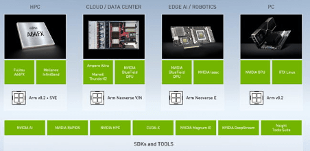
So, what does all the above have to do with packaging? 3D packaging or heterogeneous integration helps to create all of these systems. As Francoise alluded to last week in her IMAPS summary, the world is headed to chiplets. The solutions that are needed to create the hardware necessary to successfully generate the AI and ML solutions the industry is driving towards need multiple chips packaged close enough together to facilitate the operations required for the specific application. There is too much latency and not enough power when using a system-on-chip. The CPU, Neural network, GPU, and Memory chips need to be close enough together to operate at speeds faster than possible today. 3D packaging will be one of the key facilitators to make this happen.

ARM-Nvidia: Will it Work?
One of the questions surrounding the ARM Developers conference was the pending merger with Nvidia. The conference made a great pivot and had a fireside chat with the CEO of ARM Simon Segars, and Jensen Huang the CEO of Nvidia. When this merger announcement was first made, I had serious reservations. I still have concerns, but after the fireside chat, I’m a bit less concerned. I still think it will face challenges in gaining approval. In my opinion, the intellectual property (IP) that ARM provides the industry needs to be held by a neutral party i.e. something akin to Switzerland. Nvidia already uses ARM technology in the Jetson CPU and Bluefield DPU, so why not just continue on the same path to continue to improve system solutions for the data center and edge AI/ML, rather than making a $40 billion dollar purchase?
However, some of what Jensen Huang proposed during the fireside chat and then at his GTC keynote sweetens the pot and would create a much bigger IP toolset for ARM.
This expansion of additional IP into the ARM ecosystem, that then industry developers would have access to, makes the ARM/Nvidia merger much more interesting. It significantly expands the IP ARM has to offer and potentially expands the Nvidia software/hardware platform further into AI/ML applications. (This is where a virtual show falls short. It would have been interesting to see the live response from the developer community.)
This expansion of IP. if the merger gains approval, will be very interesting to watch as the edge computing space continues to grow. The ability to combine the different hardware/software technology offered into the same chip or package will give the ability to create some very specific AI/ML solutions that have yet to be imagined. I’m not sure if this will be enough to sway the decision-makers in the approval process, but it should give them some possibilities to think about as they make their decision. At the moment based upon the recent events, I am a bit more in favor of the merger taking place provided that a firewall can be created between ARM’s customers and Nvidia.


